VRAM
SMJ44C251B
MT42C4256
Austin Semiconductor, Inc.
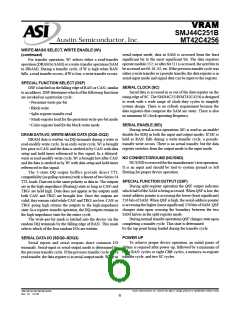
RAS\-ONLY REFRESH (continued)
all bits in each row to be refreshed. CAS\ can remain high
(inactive) for this refresh sequence to conserve power.
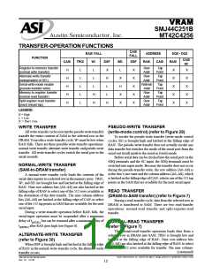
BLOCK WRITE
The block-write mode allows data (present in an on-chip
color register) to be written into four consecutive
column-address locations. The 4-bit color register is loaded by
the color-register-load cycle. Both write-per-bit modes can be
applied in the block-write cycle. The block-write mode also
offers the 4 × 4 column-mask capability.
CAS\-BEFORE-RAS\ (CBR) REFRESH
CBR refresh is accomplished by bringing CAS\ low earlier
than RAS\. The external row address is ignored and the refresh
row address is generated internally when using CBR refresh.
Other cycles can be performed in between CBR cycles without
disturbing the internal address generation.
LOAD COLOR REGISTER
The load-color-register cycle is performed using normal
DRAM write-cycle timing except that DSF is held high on the
falling edges of RAS\ and CAS\. A 4-bit code is input to the
color register via the random I/O terminals and latched on the
later of the falling edge of CAS\ or W\.After the color register is
loaded, it retains data until power is lost or until another load-
color-register cycle is executed.
HIDDEN REFRESH
A hidden refresh is accomplished by holding CAS\ low in
the DRAM-read cycle and cycling RAS\. The output data of
the DRAM-read cycle remains valid while the refresh is being
carried out. Like the CBR refresh, the refreshed row addresses
are generated internally during the hidden refresh.
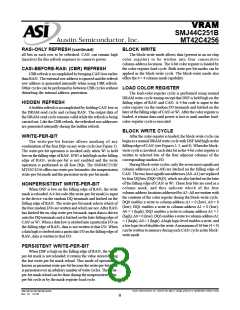
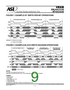
BLOCK WRITE CYCLE
After the color register is loaded, the block-write cycle can
begin as a normal DRAM write cycle with DSF held high on the
falling edge of CAS\ (see Figures 2, 3, and 4). When the block-
write cycle is invoked, each data bit in the 4-bit color register is
written to selected bits of the four adjacent columns of the
corresponding random I/O.
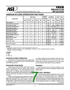
WRITE-PER-BIT
The write-per-bit feature allows masking of any
combination of the four DQs on any write cycle (see Figure 1).
The write-per-bit operation is invoked only when W\ is held
low on the falling edge of RAS\. If W\ is held high on the falling
edge of RAS\, write-per-bit is not enabled and the write
operation is performed to all four DQs. The SMJ44C251B/
MT42C4256 offers two write-per-bit modes: the nonpersistent
write-per-bit mode and the persistent write-per-bit mode.
During block-write cycles, only the seven most significant
column addresses (A2–A8) are latched on the falling edge of
CAS\. The two least significant addresses (A0–A1) are replaced
by four DQ bits (DQ0–DQ3), which are also latched on the later
of the falling edge of CAS\ or W\. These four bits are used as a
column mask, and they indicate which of the four
column-address locations addressed byA2–A8 are written with
the contents of the color register during the block-write cycle.
DQ0 enables a write to column-address A1 = 0 (low), A0 = 0
(low); DQ1 enables a write to column-address A1 = 0 (low),
A0 = 1 (high); DQ2 enables a write to column-address A1 = 1
(high),A0 = 0 (low); DQ3 enables a write to column-addressA1
= 1 (high),A0 = 1 (high).Ahigh logic level enables a write, and
a low logic level disables the write.Amaximum of 16 bits (4 × 4)
can be written to memory during each CAS\ cycle in the block-
write mode.
NONPERSISTENT WRITE-PER-BIT
When DSF is low on the falling edge of RAS\, the write
mask is reloaded.A4-bit code (the write-per-bit mask) is input
to the device via the random DQ terminals and latched on the
falling edge of RAS\. The write-per-bit mask selects which of
the four random I/Os are written and which are not. After RAS\
has latched the on-chip write-per-bit mask, input data is driven
onto the DQ terminals and is latched on the later falling edge of
CAS\ or W\. When a data low is strobed into a particular I/O on
the falling edge of RAS\, data is not written to that I/O. When
a data high is strobed into a particular I/O on the falling edge of
RAS\, data is written to that I/O.
PERSISTENT WRITE-PER-BIT
When DSF is high on the falling edge of RAS\, the write-
per-bit mask is not reloaded: it retains the value stored during
the last write-per-bit mask reload. This mode of operation is
known as persistent write-per-bit because the write-per-bit mask
is persistent over an arbitrary number of write cycles. The write-
per-bit mask reload can be done during the nonpersistent write-
per-bit cycle or by the mask-register-load cycle.
Austin Semiconductor, Inc. reserves the right to change products or specifications without notice.
SMJ44C251B/MT42C4256
Rev. 0.1 12/03
8

 AUSTIN [ AUSTIN SEMICONDUCTOR ]