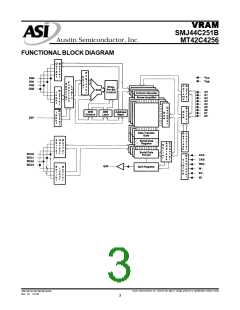
VRAM
SMJ44C251B
MT42C4256
Austin Semiconductor, Inc.
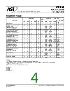
RANDOM-ACCESS-OPERATION FUNCTIONS
CAS\
FALL
RAS\ FALL
ADDRESS
DQ0 - DQ3
FUNCTION
CAS\2
W\
X
Valid
W\1
X
CAS\ TRG\
DSF
SE\
DSF
RAS\
CAS\
RAS\
CBR Refresh
L
X
H
X
L
X
X
X
L
X
Row
Addr
X
Col
Addr
X
DQ
Load and use write mask,
Write data to DRAM
Load and use write mask,
Block write to DRAM
Persistent write-per-bit,
Write data to DRAM
Persistent write-per-bit,
Block write to DRAM
Normal DRAM read/write
(nonmasked)
H
L
Mask Data
DQ Col
Mask Mask
Row Blk Addr
H
H
H
H
H
H
H
H
H
H
H
H
H
H
L
L
L
H
H
L
X
X
X
X
X
X
X
H
L
Addr
Row
Addr
A2-A8
Col
Addr
Valid
Data
Col
Mask
Valid
Data
Col
Mask
DQ
Mask
Color
Data
X
Row Blk Addr
L
H
L
X
Addr
Row
Addr
A2-A8
Col
Addr
H
H
H
H
X
Block write to DRAM
(nonmasked)
Row Blk Addr
L
H
L
X
Addr
Refresh
Addr
Refresh
Addr
A2-A8
Load write mask
H
H
X
X
Load color register
H
X
X
NOTES:
1. In persistent write-per-bit function, W must be high during the refresh cycle.
2. DQ0–DQ3 are latched on the later of W or CAS falling edge. Col Mask = H: Write to address/column location enabled.
DQ Mask = H: Write to I/O enabled
LEGEND:
H = High
L = Low
X = Don’t care
row-address hold time has been satisfied, usually well in ad-
vance of the falling edge of CAS\. In this case, data can be
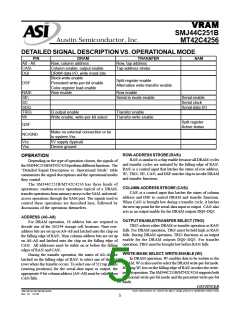
RANDOM-ACCESS OPERATION
The random-access operation functions are summarized in
the “Random-Access-Operation Function” table and described
in the following sections.
obtained after ta(C) max (access time from CAS low), if ta(CA) max
(access time from column address) has been satisfied.
ENHANCED PAGE-MODE
REFRESH
Enhanced page-mode operation allows faster memory
access by keeping the same row address while selecting
random column addresses. This mode eliminates the time
required for row address setup-and-hold and address
multiplex. The maximum RAS\ low time and the CAS\ page cycle
time used determine the number of columns that can be
accessed.
Unlike conventional page-mode operation, the enhanced
page mode allows the SMJ44C251B/MT42C4256 to operate at a
higher data bandwidth. Data retrieval begins as soon as the
column address is valid rather than when CAS\ transitions low.
A valid column address can be presented immediately after
There are three types of refresh available on the
SMJ44C251B/MT42C4256: RAS\-only refresh, CBR refresh, and
hidden refresh.
RAS\-ONLY REFRESH
A refresh operation must be performed to each row at least
once every 8 ms to retain data. Unless CAS\ is applied, the
output buffers are in the high-impedance state, so the RAS\-
only refresh sequence avoids any output during refresh. Exter-
nally generated addresses must be supplied during RAS-only
refresh. Strobing each of the 512 row addresses with RAS causes
(continued)
Austin Semiconductor, Inc. reserves the right to change products or specifications without notice.
SMJ44C251B/MT42C4256
Rev. 0.1 12/03
7

 AUSTIN [ AUSTIN SEMICONDUCTOR ]