ATmega64A
13.3.5
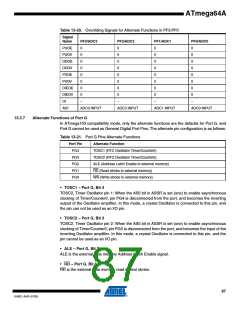
Alternate Functions of Port E
The Port E pins with alternate functions are shown in Table 13-15.
Table 13-15. Port E Pins Alternate Functions
Port Pin
PE7
Alternate Function
INT7/ICP3(1) (External Interrupt 7 Input or Timer/Counter3 Input Capture Pin)
INT6/ T3(1) (External Interrupt 6 Input or Timer/Counter3 Clock Input)
PE6
PE5
INT5/OC3C(1) (External Interrupt 5 Input or Output Compare and PWM Output C for
Timer/Counter3)
PE4
PE3
INT4/OC3B(1) (External Interrupt 4 Input or Output Compare and PWM Output B for
Timer/Counter3)
AIN1/OC3A (1) (Analog Comparator Negative Input or Output Compare and PWM Output A
for Timer/Counter3)
PE2
PE1
PE0
AIN0/XCK0(1) (Analog Comparator Positive Input or USART0 external clock input/output)
PDO/TXD0 (Programming Data Output or UART0 Transmit Pin)
PDI/RXD0 (Programming Data Input or UART0 Receive Pin)
Note:
1. ICP3, T3, OC3C, OC3B, OC3B, OC3A, and XCK0 not applicable in ATmega103 compatibility
mode.
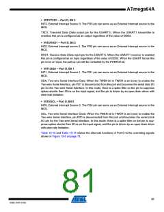
• INT7/ICP3 – Port E, Bit 7
INT7, External Interrupt Source 7: The PE7 pin can serve as an External Interrupt source.
ICP3 – Input Capture Pin3: The PE7 pin can act as an Input Capture pin for Timer/Counter3.
• INT6/T3 – Port E, Bit 6
INT6, External Interrupt Source 6: The PE6 pin can serve as an External Interrupt source.
T3, Timer/Counter3 Counter Source.
• INT5/OC3C – Port E, Bit 5
INT5, External Interrupt Source 5: The PE5 pin can serve as an External Interrupt source.
OC3C, Output Compare Match C output: The PE5 pin can serve as an external output for the
Timer/Counter3 Output Compare C. The pin has to be configured as an output (DDE5 set – one)
to serve this function. The OC3C pin is also the output pin for the PWM mode timer function.
• INT4/OC3B – Port E, Bit 4
INT4, External Interrupt Source 4: The PE4 pin can serve as an External Interrupt source.
OC3B, Output Compare Match B output: The PE4 pin can serve as an external output for the
Timer/Counter3 Output Compare B. The pin has to be configured as an output (DDE4 set – one)
to serve this function. The OC3B pin is also the output pin for the PWM mode timer function.
• AIN1/OC3A – Port E, Bit 3
AIN1 – Analog Comparator Negative input. This pin is directly connected to the negative input of
the Analog Comparator.
OC3A, Output Compare Match A output: The PE3 pin can serve as an external output for the
Timer/Counter3 Output Compare A. The pin has to be configured as an output (DDE3 set – one)
to serve this function. The OC3A pin is also the output pin for the PWM mode timer function.
83
8160C–AVR–07/09

 ATMEL [ ATMEL ]