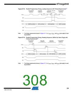
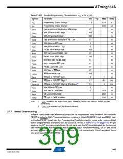
ATmega64A
27.8.3
Data Polling EEPROM
When a new byte has been written and is being programmed into EEPROM, reading the
address location being programmed will give the value 0xFF. At the time the device is ready for
a new byte, the programmed value will read correctly. This is used to determine when the next
byte can be written. This will not work for the value 0xFF, but the user should have the following
in mind: As a chip erased device contains 0xFF in all locations, programming of addresses that
are meant to contain 0xFF, can be skipped. This does not apply if the EEPROM is re-pro-
grammed without chip erasing the device. In this case, data polling cannot be used for the value
0xFF, and the user will have to wait at least tWD_EEPROM before programming the next byte. See
Table 27-14 for tWD_EEPROM value.
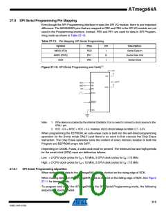
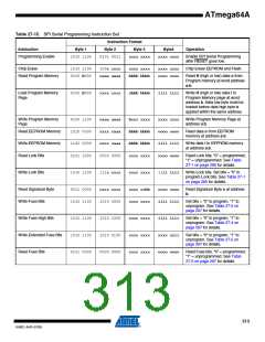
Table 27-14. Minimum Wait Delay before Writing the Next Flash or EEPROM Location
Symbol
tWD_FUSE
tWD_FLASH
Minimum Wait Delay
4.5 ms
(1)
4.5 ms
tWD_EEPROM
tWD_ERASE
9.0 ms
9.0 ms
Note:
1. Flash write: per page
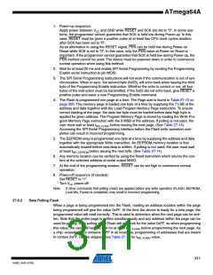
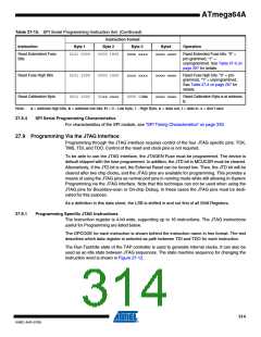
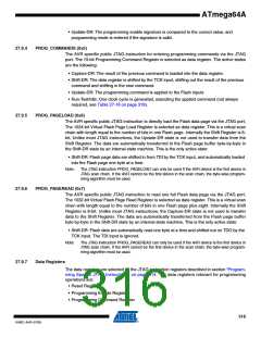
Figure 27-11. SPI Serial Programming Waveforms
SERIAL DATA INPUT
(MOSI)
MSB
MSB
LSB
LSB
SERIAL DATA OUTPUT
(MISO)
SERIAL CLOCK INPUT
(SCK)
SAMPLE
312
8160C–AVR–07/09

 ATMEL [ ATMEL ]