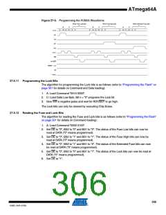
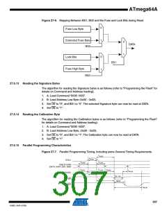
ATmega64A
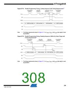
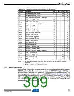
Table 27-12. Parallel Programming Characteristics, VCC = 5V 10%
Symbol
VPP
Parameter
Min
Typ
Max
12.5
250
Units
V
Programming Enable Voltage
Programming Enable Current
Data and Control Valid before XTAL1 High
XTAL1 Low to XTAL1 High
XTAL1 Pulse Width High
Data and Control Hold after XTAL1 Low
XTAL1 Low to WR Low
11.5
IPP
μA
ns
ns
ns
ns
ns
ns
ns
ns
ns
ns
ns
ns
ns
ns
μs
ms
ms
ns
ns
ns
ns
tDVXH
tXLXH
tXHXL
tXLDX
tXLWL
tXLPH
tPLXH
tBVPH
tPHPL
tPLBX
tWLBX
tPLWL
tBVWL
tWLWH
tWLRL
tWLRH
tWLRH_CE
tXLOL
tBVDV
tOLDV
tOHDZ
67
200
150
67
0
XTAL1 Low to PAGEL high
PAGEL low to XTAL1 high
BS1 Valid before PAGEL High
PAGEL Pulse Width High
BS1 Hold after PAGEL Low
BS2/1 Hold after WR Low
PAGEL Low to WR Low
0
150
67
150
67
67
67
67
150
0
BS1 Valid to WR Low
WR Pulse Width Low
WR Low to RDY/BSY Low
WR Low to RDY/BSY High(1)
WR Low to RDY/BSY High for Chip Erase(2)
XTAL1 Low to OE Low
1
4.5
9
3.7
7.5
0
BS1 Valid to DATA valid
0
250
250
250
OE Low to DATA Valid
OE High to DATA Tri-stated
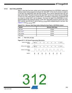
Note:
1. tWLRH is valid for the Write Flash, Write EEPROM, Write Fuse Bits and Write Lock bits
commands.
2.
tWLRH_CE is valid for the Chip Erase command.
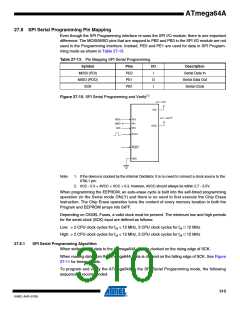
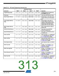
27.7 Serial Downloading
Both the Flash and EEPROM memory arrays can be programmed using the serial SPI bus while
RESET is pulled to GND. The serial interface consists of pins SCK, MOSI (input) and MISO (out-
put). After RESET is set low, the Programming Enable instruction needs to be executed first
before program/erase operations can be executed. NOTE, in Table 27-13 on page 310, the pin
mapping for SPI programming is listed. Not all parts use the SPI pins dedicated for the internal
SPI interface. Note that throughout the description about Serial downloading, MOSI and MISO
are used to describe the serial data in and serial data out, respectively. For ATmega64A, these
pins are mapped to PDI and PDO.
309
8160C–AVR–07/09

 ATMEL [ ATMEL ]