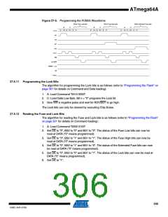
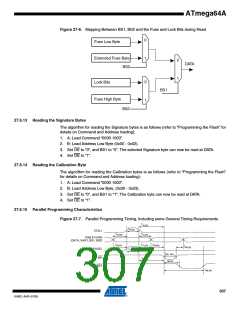
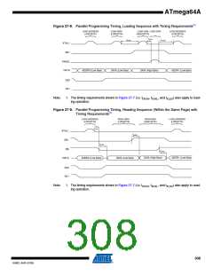
ATmega64A
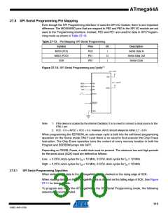
27.8 SPI Serial Programming Pin Mapping
Even though the SPI Programming interface re-uses the SPI I/O module, there is one important
difference: The MOSI/MISO pins that are mapped to PB2 and PB3 in the SPI I/O module are not
used in the Programming interface. Instead, PE0 and PE1 are used for data in SPI Program-
ming mode as shown in Table 27-13.
Table 27-13. Pin Mapping SPI Serial Programming
Symbol
MOSI (PDI)
MISO (PDO)
SCK
Pins
PE0
PE1
PB1
I/O
Description
Serial Data In
Serial Data Out
Serial Clock
I
O
I
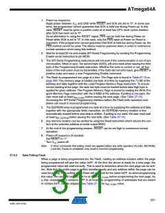
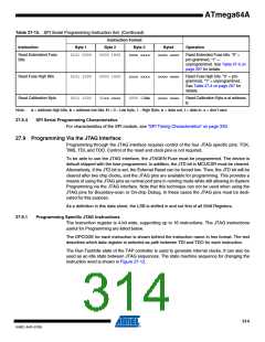
Figure 27-10. SPI Serial Programming and Verify(1)
+2.7 - 5.5V
VCC
+2.7 - 5.5V (2)
PE0
PE1
PB1
MOSI
MISO
AVCC
SCK
XTAL1
RESET
GND
Note:
1. If the device is clocked by the internal Oscillator, it is no need to connect a clock source to the
XTAL1 pin.
2. VCC - 0.3 < AVCC < VCC + 0.3, however, AVCC should always be within 2.7 - 5.5V.
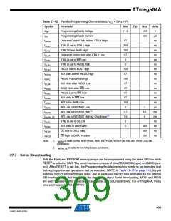
When programming the EEPROM, an auto-erase cycle is built into the self-timed programming
operation (in the Serial mode ONLY) and there is no need to first execute the Chip Erase
instruction. The Chip Erase operation turns the content of every memory location in both the
Program and EEPROM arrays into 0xFF.
Depending on CKSEL Fuses, a valid clock must be present. The minimum low and high periods
for the serial clock (SCK) input are defined as follows:
Low: > 2 CPU clock cycles for fck < 12 MHz, 3 CPU clock cycles for fck 12 MHz
High: > 2 CPU clock cycles for fck < 12 MHz, 3 CPU clock cycles for fck 12 MHz
27.8.1
SPI Serial Programming Algorithm
When writing serial data to the ATmega64A, data is clocked on the rising edge of SCK.
When reading data from the ATmega64A, data is clocked on the falling edge of SCK. See Figure
27-11 for timing details.
To program and verify the ATmega64A in the SPI Serial Programming mode, the following
sequence is recommended:
310
8160C–AVR–07/09

 ATMEL [ ATMEL ]