ATmega64A
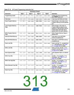
Table 27-15. SPI Serial Programming Instruction Set (Continued)
Instruction Format
Instruction
Byte 1
Byte 2
Byte 3
Byte4
Operation
Read Extendend Fuse
Bits
0101 0000
0000 1000
xxxx xxxx
oooo oooo
Read Extended Fuse bits. “0” =
pro-grammed, “1” =
unprogrammed. See Table 27-5 on
page 297 for details.
Read Fuse High Bits
Read Calibration Byte
0101 1000
0011 1000
0000 1000
00xx xxxx
xxxx xxxx
oooo oooo
oooo oooo
Read Fuse high bits. “0” = pro-
grammed, “1” = unprogrammed.
See Table 27-4 on page 297 for
details.
0000 00bb
Read Calibration Byte o at address
b.
Note:
a = address high bits, b = address low bits, H = 0 - Low byte, 1 - High Byte, o = data out, i = data in, x = don’t care
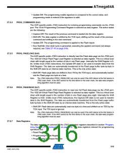
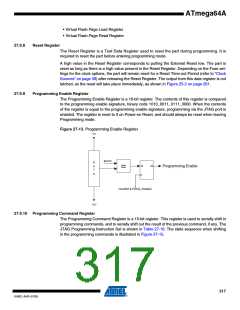
27.8.4
SPI Serial Programming Characteristics
For characteristics of the SPI module, see “SPI Timing Characteristics” on page 333.
27.9 Programming Via the JTAG Interface
Programming through the JTAG interface requires control of the four JTAG specific pins: TCK,
TMS, TDI, and TDO. Control of the reset and clock pins is not required.
To be able to use the JTAG interface, the JTAGEN Fuse must be programmed. The device is
default shipped with the fuse programmed. In addition, the JTD bit in MCUCSR must be cleared.
Alternatively, if the JTD bit is set, the External Reset can be forced low. Then, the JTD bit will be
cleared after two chip clocks, and the JTAG pins are available for programming. This provides a
means of using the JTAG pins as normal port pins in running mode while still allowing In-System
Programming via the JTAG interface. Note that this technique can not be used when using the
JTAG pins for Boundary-scan or On-chip Debug. In these cases the JTAG pins must be dedi-
cated for this purpose.
As a definition in this data sheet, the LSB is shifted in and out first of all Shift Registers.
27.9.1
Programming Specific JTAG Instructions
The instruction register is 4-bit wide, supporting up to 16 instructions. The JTAG instructions
useful for Programming are listed below.
The OPCODE for each instruction is shown behind the instruction name in hex format. The text
describes which data register is selected as path between TDI and TDO for each instruction.
The Run-Test/Idle state of the TAP controller is used to generate internal clocks. It can also be
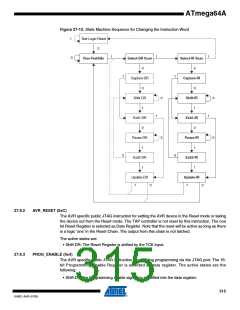
used as an idle state between JTAG sequences. The state machine sequence for changing the
instruction word is shown in Figure 27-12.
314
8160C–AVR–07/09

 ATMEL [ ATMEL ]