ATmega64A
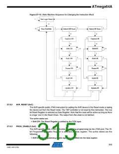
1. Power-up sequence:
Apply power between VCC and GND while RESET and SCK are set to “0”. In some sys-
tems, the programmer cannot guarantee that SCK is held low during Power-up. In this
case, RESET must be given a positive pulse of at least two CPU clock cycles duration
after SCK has been set to “0”.
As an alternative to using the RESET signal, PEN can be held low during Power-on
Reset while SCK is set to “0”. In this case, only the PEN value at Power-on Reset is
important. If the programmer cannot guarantee that SCK is held low during Power-up, the
PEN method cannot be used. The device must be powered down in order to commence
normal operation when using this method.
2. Wait for at least 20 ms and enable SPI Serial Programming by sending the Programming
Enable serial instruction to pin MOSI.
3. The SPI Serial Programming instructions will not work if the communication is out of syn-
chronization. When in sync. the second byte (0x53), will echo back when issuing the third
byte of the Programming Enable instruction. Whether the echo is correct or not, all four
bytes of the instruction must be transmitted. If the 0x53 did not echo back, give RESET a
positive pulse and issue a new Programming Enable command.
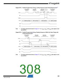
4. The Flash is programmed one page at a time. The Page size is found in Table 27-10 on
page 300. The memory page is loaded one byte at a time by supplying the 7 LSB of the
address and data together with the Load Program Memory Page instruction. To ensure
correct loading of the page, the data low byte must be loaded before data high byte is
applied for given address. The Program Memory Page is stored by loading the Write Pro-
gram Memory Page instruction with the 8 MSB of the address. If polling is not used, the
user must wait at least tWD_FLASH before issuing the next page. (See Table 27-14).
Accessing the SPI Serial Programming interface before the Flash write operation com-
pletes can result in incorrect programming.
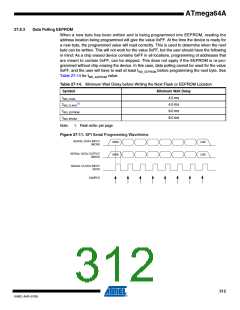
5. The EEPROM array is programmed one byte at a time by supplying the address and data
together with the appropriate Write instruction. An EEPROM memory location is first
automatically erased before new data is written. If polling is not used, the user must wait
at least tWD_EEPROM before issuing the next byte. (See Table 27-14).
6. Any memory location can be verified by using the Read instruction which returns the con-
tent at the selected address at serial output MISO.
7. At the end of the programming session, RESET can be set high to commence normal
operation.
8. Power-off sequence (if needed):
Set RESET to “1”.
Turn VCC power off.
Note:
If other commands that polling (read) are applied before any write operation (FLASH, EEPROM,
Lock bits, Fuses) is completed, may result in incorrect programming.
27.8.2
Data Polling Flash
When a page is being programmed into the Flash, reading an address location within the page
being programmed will give the value 0xFF. At the time the device is ready for a new page, the
programmed value will read correctly. This is used to determine when the next page can be writ-
ten. Note that the entire page is written simultaneously and any address within the page can be
used for polling. Data polling of the Flash will not work for the value 0xFF, so when programming
this value, the user will have to wait for at least tWD_FLASH before programming the next page. As
a chip -erased device contains 0xFF in all locations, programming of addresses that are meant
to contain 0xFF, can be skipped. See Table 27-14 for tWD_FLASH value.
311
8160C–AVR–07/09

 ATMEL [ ATMEL ]