ATmega64A
• Update-DR: The programming enable signature is compared to the correct value, and
programming mode is entered if the signature is valid.
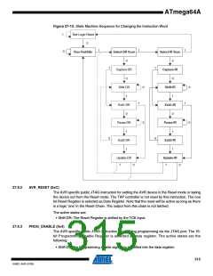
27.9.4
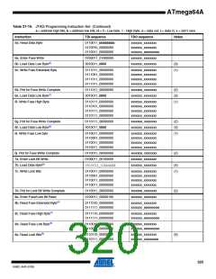
PROG_COMMANDS (0x5)
The AVR specific public JTAG instruction for entering programming commands via the JTAG
port. The 15-bit Programming Command Register is selected as data register. The active states
are the following:
• Capture-DR: The result of the previous command is loaded into the data register.
• Shift-DR: The data register is shifted by the TCK input, shifting out the result of the previous
command and shifting in the new command.
• Update-DR: The programming command is applied to the Flash inputs
• Run-Test/Idle: One clock cycle is generated, executing the applied command (not always
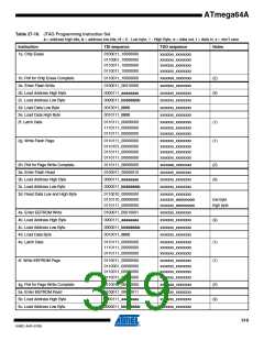
required, see Table 27-16 on page 319).
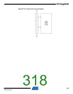
27.9.5
PROG_PAGELOAD (0x6)
The AVR specific public JTAG instruction to directly load the Flash data page via the JTAG port.
The 1024-bit Virtual Flash Page Load Register is selected as data register. This is a virtual scan
chain with length equal to the number of bits in one Flash page. Internally the Shift Register is 8-
bit. Unlike most JTAG instructions, the Update-DR state is not used to transfer data from the
Shift Register. The data are automatically transferred to the Flash page buffer byte-by-byte in
the Shift-DR state by an internal state machine. This is the only active state:
• Shift-DR: Flash page data are shifted in from TDI by the TCK input, and automatically loaded
into the Flash page one byte at a time.
Note:
The JTAG instruction PROG_PAGELOAD can only be used if the AVR device is the first device in
JTAG scan chain. If the AVR cannot be the first device in the scan chain, the byte-wise program-
ming algorithm must be used.
27.9.6
PROG_PAGEREAD (0x7)
The AVR specific public JTAG instruction to read one full Flash data page via the JTAG port.
The 1032-bit Virtual Flash Page Read Register is selected as data register. This is a virtual scan
chain with length equal to the number of bits in one Flash page plus eight. Internally the Shift
Register is 8-bit. Unlike most JTAG instructions, the Capture-DR state is not used to transfer
data to the Shift Register. The data are automatically transferred from the Flash page buffer
byte-by-byte in the Shift-DR state by an internal state machine. This is the only active state:
• Shift-DR: Flash data are automatically read one byte at a time and shifted out on TDO by the
TCK input. The TDI input is ignored.
Note:
The JTAG instruction PROG_PAGEREAD can only be used if the AVR device is the first device in
JTAG scan chain. If the AVR cannot be the first device in the scan chain, the byte-wise program-
ming algorithm must be used.
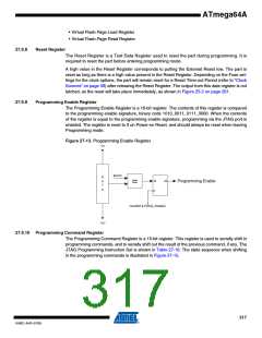
27.9.7
Data Registers
The data registers are selected by the JTAG instruction registers described in section “Program-
ming Specific JTAG Instructions” on page 314. The data registers relevant for programming
operations are:
• Reset Register
• Programming Enable Register
• Programming Command Register
316
8160C–AVR–07/09

 ATMEL [ ATMEL ]