ATmega64A
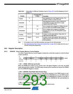
Table 27-4. Fuse High Byte
Fuse High Byte
Bit no
Description
Default Value
OCDEN
7
Enable OCD
1 (unprogrammed, OCD
disabled)
JTAGEN(4)
SPIEN(1)
6
5
Enable JTAG
0 (programmed, JTAG
enabled)
Enable SPI Serial Program and Data
Downloading
0 (programmed, SPI prog.
enabled)
CKOPT(2)
EESAVE
4
3
Oscillator options
1 (unprogrammed)
EEPROM memory is preserved
through the Chip Erase
1 (unprogrammed, EEPROM
not preserved)
BOOTSZ1
BOOTSZ0
BOOTRST
2
1
0
Select Boot Size (see Table 26-6 for
details)
0 (programmed)(3)
0 (programmed)(3)
1 (unprogrammed)
Select Boot Size (see Table 26-6 for
details)
Select Reset Vector
Note:
1. The SPIEN Fuse is not accessible in SPI Serial Programming mode.
2. The CKOPT Fuse functionality depends on the setting of the CKSEL bits. See “Clock
Sources” on page 38 for details.
3. The default value of BOOTSZ1:0 results in maximum Boot Size. See Table 26-6 on page 292
4. If the JTAG interface is left unconnected, the JTAGEN fuse should if possible be disabled. This
to avoid static current at the TDO pin in the JTAG interface
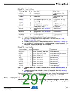
Table 27-5. Fuse Low Byte
Fuse Low Byte
BODLEVEL
BODEN
Bit no
Description
Default Value
7
6
5
4
3
2
1
0
Brown out detector trigger level
Brown out detector enable
Select start-up time
Select start-up time
Select Clock source
Select Clock source
Select Clock source
Select Clock source
1 (unprogrammed)
1 (unprogrammed, BOD disabled)
1 (unprogrammed)(1)
0 (programmed)(1)
SUT1
SUT0
CKSEL3
CKSEL2
CKSEL1
CKSEL0
0 (programmed)(2)
0 (programmed)(2)
0 (programmed)(2)
1 (unprogrammed)(2)
Note:
1. The default value of SUT1:0 results in maximum start-up time. See Table 8-8 on page 42 for
details.
2. The default setting of CKSEL3:0 results in internal RC Oscillator @ 1 MHz. See Table 8-1 on
page 38 for details.
The status of the Fuse bits is not affected by Chip Erase. Note that the Fuse bits are locked if
Lock bit1 (LB1) is programmed. Program the Fuse bits before programming the Lock bits.
27.2.1
Latching of Fuses
The fuse values are latched when the device enters Programming mode and changes of the
fuse values will have no effect until the part leaves Programming mode. This does not apply to
297
8160C–AVR–07/09

 ATMEL [ ATMEL ]