ATmega64A
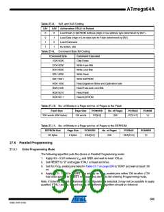
1. Set Prog_enable pins listed in Table on page 299 to “0000”.
2. Apply 4.5 - 5.5V between VCC and GND simultaneously as 11.5 - 12.5V is applied to
RESET.
3. Wait 100 µs.
4. Re-program the fuses to ensure that External Clock is selected as clock source
(CKSEL3:0 = 0b0000) If Lock bits are programmed, a Chip Erase command must be
executed before changing the fuses.
5. Exit Programming mode by power the device down or by bringing RESET pin to 0b0.
6. Entering Programming mode with the original algorithm, as described above.
27.6.2
Considerations for Efficient Programming
The loaded command and address are retained in the device during programming. For efficient
programming, the following should be considered.
•
•
•
The command needs only be loaded once when writing or reading multiple memory
locations.
Skip writing the data value 0xFF, that is the contents of the entire EEPROM (unless the
EESAVE Fuse is programmed) and Flash after a Chip Erase.
Address high byte needs only be loaded before programming or reading a new 256 word
window in Flash or 256 byte EEPROM. This consideration also applies to Signature bytes
reading.
27.6.3
Chip Erase
The Chip Erase will erase the Flash and EEPROM(1) memories plus Lock bits. The Lock bits are
not reset until the program memory has been completely erased. The Fuse bits are not
changed. A Chip Erase must be performed before the Flash and/or the EEPROM
reprogrammed.
Note:
1. The EEPRPOM memory is preserved during chip erase if the EESAVE Fuse is programmed.
Load Command “Chip Erase”
1. Set XA1, XA0 to “10”. This enables command loading.
2. Set BS1 to “0”.
3. Set DATA to “1000 0000”. This is the command for Chip Erase.
4. Give XTAL1 a positive pulse. This loads the command.
5. Give WR a negative pulse. This starts the Chip Erase. RDY/BSY goes low.
6. Wait until RDY/BSY goes high before loading a new command.
27.6.4
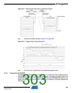
Programming the Flash
The Flash is organized in pages, see Table 27-9 on page 300. When programming the Flash,
the program data is latched into a page buffer. This allows one page of program data to be pro-
grammed simultaneously. The following procedure describes how to program the entire Flash
memory:
A. Load Command “Write Flash”
1. Set XA1, XA0 to “10”. This enables command loading.
2. Set BS1 to “0”.
3. Set DATA to “0001 0000”. This is the command for Write Flash.
4. Give XTAL1 a positive pulse. This loads the command.
301
8160C–AVR–07/09

 ATMEL [ ATMEL ]