ATmega64A
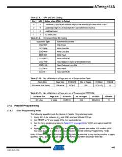
Table 27-8. XA1 and XA0 Coding
XA1
XA0
Action when XTAL1 is Pulsed
0
0
1
1
0
1
0
1
Load Flash or EEPROM Address (High or low address byte determined by BS1)
Load Data (High or Low data byte for Flash determined by BS1)
Load Command
No Action, Idle
Table 27-9. Command Byte Bit Coding
Command Byte
1000 0000
0100 0000
0010 0000
0001 0000
0001 0001
0000 1000
0000 0100
0000 0010
0000 0011
Command Executed
Chip Erase
Write Fuse Bits
Write Lock Bits
Write Flash
Write EEPROM
Read Signature Bytes and Calibration byte
Read Fuse and Lock Bits
Read Flash
Read EEPROM
Table 27-10. No. of Words in a Page and no. of Pages in the Flash
Flash Size
Page Size
PCWORD
No. of Pages
PCPAGE
PCMSB
32K words (64K bytes)
128 words
PC[6:0]
256
PC[14:7]
14
Table 27-11. No. of Words in a Page and no. of Pages in the EEPROM
EEPROM Size
Page Size
PCWORD
No. of Pages
PCPAGE
EEA[10:3]
EEAMSB
2K bytes
8 bytes
EEA[2:0]
256
10
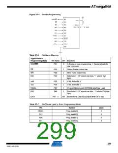
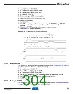
27.6 Parallel Programming
27.6.1
Enter Programming Mode
The following algorithm puts the device in Parallel Programming mode:
1. Apply 4.5 - 5.5V between VCC and GND, and wait at least 100 µs.
2. Set RESET to “0” and toggle XTAL1 at least six times.
3. Set the Prog_enable pins listed in Table 27-7 on page 299 to “0000” and wait at least 100
ns.
4. Apply 11.5 - 12.5V to RESET. Any activity on Prog_enable pins within 100 ns after +12V
has been applied to RESET, will cause the device to fail entering Programming mode.
Note, if External Crystal or External RC configuration is selected, it may not be possible to apply
qualified XTAL1 pulses. In such cases, the following algorithm should be followed:
300
8160C–AVR–07/09

 ATMEL [ ATMEL ]