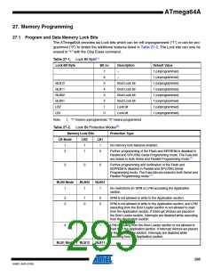
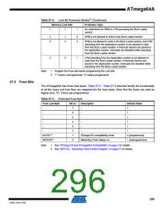
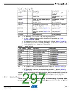
ATmega64A
the EESAVE Fuse which will take effect once it is programmed. The fuses are also latched on
Power-up in Normal mode.
27.3 Signature Bytes
All Atmel microcontrollers have a 3-byte signature code which identifies the device. This code
can be read in both Serial and Parallel mode, also when the device is locked. The three bytes
reside in a separate address space.
For the ATmega64A the signature bytes are:
1. 0x000: 0x1E (indicates manufactured by Atmel)
2. 0x001: 0x96 (indicates 64KB Flash memory)
3. 0x002: 0x02 (indicates ATmega64A device when 0x001 is 0x96)
27.4 Calibration Byte
The ATmega64A stores four different calibration values for the internal RC Oscillator. These
bytes resides in the signature row high byte of the addresses 0x000, 0x0001, 0x0002, and
0x0003 for 1, 2, 4, and 8 MHz respectively. During Reset, the 1 MHz value is automatically
loaded into the OSCCAL Register. If other frequencies are used, the calibration value has to be
loaded manually, see “OSCCAL – Oscillator Calibration Register(1)” on page 44 for details.
27.5 Parallel Programming Parameters, Pin Mapping, and Commands
This section describes how to parallel program and verify Flash Program memory, EEPROM
Data memory, Memory Lock bits, and Fuse bits in the ATmega64A. Pulses are assumed to be at
least 250 ns unless otherwise noted.
27.5.1
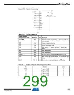
Signal Names
In this section, some pins of the ATmega64A are referenced by signal names describing their
functionality during parallel programming, see Figure 27-1 and Table 27-6. Pins not described in
the following table are referenced by pin names.
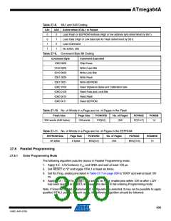
The XA1/XA0 pins determine the action executed when the XTAL1 pin is given a positive pulse.
The bit coding is shown in Table 27-8.
When pulsing WR or OE, the command loaded determines the action executed. The different
Commands are shown in Table 27-9.
298
8160C–AVR–07/09

 ATMEL [ ATMEL ]