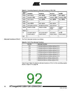
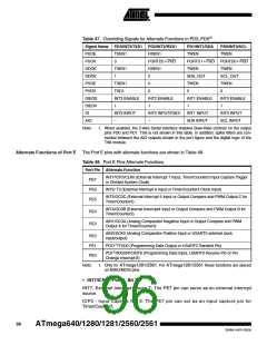
Alternate Functions of Port D The Port D pins with alternate functions are shown in Table 45.
Table 45. Port D Pins Alternate Functions
Port Pin
PD7
Alternate Function
T0 (Timer/Counter0 Clock Input)
PD6
T1 (Timer/Counter1 Clock Input)
PD5
XCK1 (USART1 External Clock Input/Output)
ICP1 (Timer/Counter1 Input Capture Trigger)
INT3/TXD1 (External Interrupt3 Input or USART1 Transmit Pin)
INT2/RXD1 (External Interrupt2 Input or USART1 Receive Pin)
INT1/SDA (External Interrupt1 Input or TWI Serial DAta)
INT0/SCL (External Interrupt0 Input or TWI Serial CLock)
PD4
PD3
PD2
PD1
PD0
The alternate pin configuration is as follows:
• T0 – Port D, Bit 7
T0, Timer/Counter0 counter source.
• T1 – Port D, Bit 6
T1, Timer/Counter1 counter source.
• XCK1 – Port D, Bit 5
XCK1, USART1 External clock. The Data Direction Register (DDD5) controls whether
the clock is output (DDD5 set) or input (DDD5 cleared). The XCK1 pin is active only
when the USART1 operates in Synchronous mode.
• ICP1 – Port D, Bit 4
ICP1 – Input Capture Pin 1: The PD4 pin can act as an input capture pin for
Timer/Counter1.
• INT3/TXD1 – Port D, Bit 3
INT3, External Interrupt source 3: The PD3 pin can serve as an external interrupt source
to the MCU.
TXD1, Transmit Data (Data output pin for the USART1). When the USART1 Transmitter
is enabled, this pin is configured as an output regardless of the value of DDD3.
• INT2/RXD1 – Port D, Bit 2
INT2, External Interrupt source 2. The PD2 pin can serve as an External Interrupt
source to the MCU.
RXD1, Receive Data (Data input pin for the USART1). When the USART1 receiver is
enabled this pin is configured as an input regardless of the value of DDD2. When the
USART forces this pin to be an input, the pull-up can still be controlled by the PORTD2
bit.
94
ATmega640/1280/1281/2560/2561
2549A–AVR–03/05

 ATMEL [ ATMEL ]