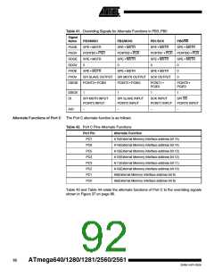
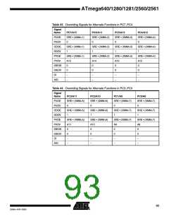
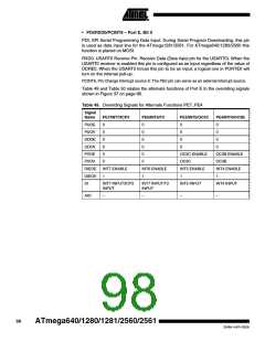
Table 47. Overriding Signals for Alternate Functions in PD3..PD0(1)
Signal Name PD3/INT3/TXD1 PD2/INT2/RXD1
PD1/INT1/SDA
PD0/INT0/SCL
PUOE
PUOV
DDOE
DDOV
PVOE
PVOV
DIEOE
DIEOV
DI
TXEN1
RXEN1
TWEN
TWEN
0
PORTD2 • PUD
PORTD1 • PUD PORTD0 • PUD
TXEN1
RXEN1
TWEN
TWEN
1
0
SDA_OUT
SCL_OUT
TWEN
TXEN1
0
TWEN
TXD1
0
0
0
INT3 ENABLE
INT2 ENABLE
1
INT1 ENABLE
1
INT0 ENABLE
1
1
INT3 INPUT
–
INT2 INPUT/RXD1 INT1 INPUT
– SDA INPUT
INT0 INPUT
SCL INPUT
AIO
Note:
1. When enabled, the 2-wire Serial Interface enables Slew-Rate controls on the output
pins PD0 and PD1. This is not shown in this table. In addition, spike filters are con-
nected between the AIO outputs shown in the port figure and the digital logic of the
TWI module.
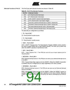
Alternate Functions of Port E
The Port E pins with alternate functions are shown in Table 48.
Table 48. Port E Pins Alternate Functions
Port Pin Alternate Function
INT7/ICP3/CLK0 (External Interrupt 7 Input, Timer/Counter3 Input Capture Trigger
or Divided System Clock)
PE7
PE6
PE5
INT6/ T3 (External Interrupt 6 Input or Timer/Counter3 Clock Input)
INT5/OC3C (External Interrupt 5 Input or Output Compare and PWM Output C for
Timer/Counter3)
INT4/OC3B (External Interrupt4 Input or Output Compare and PWM Output B for
Timer/Counter3)
PE4
PE3
AIN1/OC3A (Analog Comparator Negative Input or Output Compare and PWM
Output A for Timer/Counter3)
AIN0/XCK0 (Analog Comparator Positive Input or USART0 external clock
input/output)
PE2
PE1
PE0
PDO(1)/TXD0 (Programming Data Output or USART0 Transmit Pin)
PDI(1)/RXD0/PCINT8 (Programming Data Input, USART0 Receive Pin or Pin
Change Interrupt 8)
Note:
1. Only for ATmega1281/2561. For ATmega1281/2561 these functions are placed
on MISO/MOSI pins.
• INT7/ICP3 – Port E, Bit 7
INT7, External Interrupt source 7: The PE7 pin can serve as an external interrupt
source.
ICP3 - Input Capture Pin 3: The PE7 pin can act as an input capture pin for
Timer/Counter3.
96
ATmega640/1280/1281/2560/2561
2549A–AVR–03/05

 ATMEL [ ATMEL ]