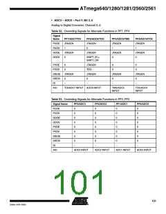
ATmega640/1280/1281/2560/2561
CLKO - Divided System Clock: The divided system clock can be output on the PE7 pin.
The divided system clock will be output if the CKOUT Fuse is programmed, regardless
of the PORTE7 and DDE7 settings. It will also be output during reset.
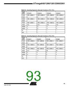
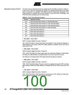
• INT6/T3 – Port E, Bit 6
INT6, External Interrupt source 6: The PE6 pin can serve as an external interrupt
source.
T3, Timer/Counter3 counter source.
• INT5/OC3C – Port E, Bit 5
INT5, External Interrupt source 5: The PE5 pin can serve as an External Interrupt
source.
OC3C, Output Compare Match C output: The PE5 pin can serve as an External output
for the Timer/Counter3 Output Compare C. The pin has to be configured as an output
(DDE5 set “one”) to serve this function. The OC3C pin is also the output pin for the
PWM mode timer function.
• INT4/OC3B – Port E, Bit 4
INT4, External Interrupt source 4: The PE4 pin can serve as an External Interrupt
source.
OC3B, Output Compare Match B output: The PE4 pin can serve as an External output
for the Timer/Counter3 Output Compare B. The pin has to be configured as an output
(DDE4 set (one)) to serve this function. The OC3B pin is also the output pin for the PWM
mode timer function.
• AIN1/OC3A – Port E, Bit 3
AIN1 – Analog Comparator Negative input. This pin is directly connected to the negative
input of the Analog Comparator.
OC3A, Output Compare Match A output: The PE3 pin can serve as an External output
for the Timer/Counter3 Output Compare A. The pin has to be configured as an output
(DDE3 set “one”) to serve this function. The OC3A pin is also the output pin for the PWM
mode timer function.
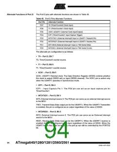
• AIN0/XCK0 – Port E, Bit 2
AIN0 – Analog Comparator Positive input. This pin is directly connected to the positive
input of the Analog Comparator.
XCK0, USART0 External clock. The Data Direction Register (DDE2) controls whether
the clock is output (DDE2 set) or input (DDE2 cleared). The XCK0 pin is active only
when the USART0 operates in Synchronous mode.
• PDO/TXD0 – Port E, Bit 1
PDO, SPI Serial Programming Data Output. During Serial Program Downloading, this
pin is used as data output line for the ATmega1281/2561. For ATmega640/1280/2560
this function is placed on MISO.
TXD0, USART0 Transmit pin.
97
2549A–AVR–03/05

 ATMEL [ ATMEL ]