ATmega640/1280/1281/2560/2561
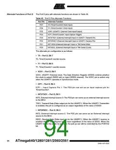
• INT1/SDA – Port D, Bit 1
INT1, External Interrupt source 1. The PD1 pin can serve as an external interrupt source
to the MCU.
SDA, 2-wire Serial Interface Data: When the TWEN bit in TWCR is set (one) to enable
the 2-wire Serial Interface, pin PD1 is disconnected from the port and becomes the
Serial Data I/O pin for the 2-wire Serial Interface. In this mode, there is a spike filter on
the pin to suppress spikes shorter than 50 ns on the input signal, and the pin is driven by
an open drain driver with slew-rate limitation.
• INT0/SCL – Port D, Bit 0
INT0, External Interrupt source 0. The PD0 pin can serve as an external interrupt source
to the MCU.
SCL, 2-wire Serial Interface Clock: When the TWEN bit in TWCR is set (one) to enable
the 2-wire Serial Interface, pin PD0 is disconnected from the port and becomes the
Serial Clock I/O pin for the 2-wire Serial Interface. In this mode, there is a spike filter on
the pin to suppress spikes shorter than 50 ns on the input signal, and the pin is driven by
an open drain driver with slew-rate limitation.
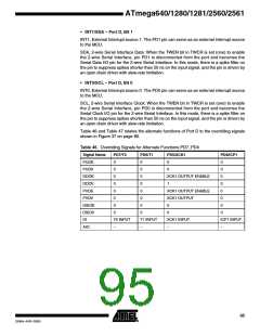
Table 46 and Table 47 relates the alternate functions of Port D to the overriding signals
shown in Figure 37 on page 86.
Table 46. Overriding Signals for Alternate Functions PD7..PD4
Signal Name
PUOE
PUOV
DDOE
DDOV
PVOE
PVOV
DIEOE
DIEOV
DI
PD7/T0
PD6/T1
PD5/XCK1
PD4/ICP1
0
0
0
0
0
0
0
0
0
0
XCK1 OUTPUT ENABLE
0
0
0
1
0
0
0
XCK1 OUTPUT ENABLE
0
0
0
XCK1 OUTPUT
0
0
0
0
0
0
0
0
0
T0 INPUT
–
T1 INPUT
–
XCK1 INPUT
–
ICP1 INPUT
–
AIO
95
2549A–AVR–03/05

 ATMEL [ ATMEL ]