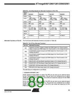
PCINT7, Pin Change Interrupt source 7: The PB7 pin can serve as an external interrupt
source.
• OC1B/PCINT6, Bit 6
OC1B, Output Compare Match B output: The PB6 pin can serve as an external output
for the Timer/Counter1 Output Compare B. The pin has to be configured as an output
(DDB6 set (one)) to serve this function. The OC1B pin is also the output pin for the PWM
mode timer function.
PCINT6, Pin Change Interrupt source 6: The PB7 pin can serve as an external interrupt
source.
• OC1A/PCINT5, Bit 5
OC1A, Output Compare Match A output: The PB5 pin can serve as an external output
for the Timer/Counter1 Output Compare A. The pin has to be configured as an output
(DDB5 set (one)) to serve this function. The OC1A pin is also the output pin for the PWM
mode timer function.
PCINT5, Pin Change Interrupt source 5: The PB7 pin can serve as an external interrupt
source.
• OC2A/PCINT4, Bit 4
OC2A, Output Compare Match output: The PB4 pin can serve as an external output for
the Timer/Counter2 Output Compare. The pin has to be configured as an output (DDB4
set (one)) to serve this function. The OC2A pin is also the output pin for the PWM mode
timer function.
PCINT4, Pin Change Interrupt source 4: The PB7 pin can serve as an external interrupt
source.
• MISO/PCINT3 – Port B, Bit 3
MISO: Master Data input, Slave Data output pin for SPI channel. When the SPI is
enabled as a master, this pin is configured as an input regardless of the setting of
DDB3. When the SPI is enabled as a slave, the data direction of this pin is controlled by
DDB3. When the pin is forced to be an input, the pull-up can still be controlled by the
PORTB3 bit.
PCINT3, Pin Change Interrupt source 3: The PB7 pin can serve as an external interrupt
source.
• MOSI/PCINT2 – Port B, Bit 2
MOSI: SPI Master Data output, Slave Data input for SPI channel. When the SPI is
enabled as a slave, this pin is configured as an input regardless of the setting of DDB2.
When the SPI is enabled as a master, the data direction of this pin is controlled by
DDB2. When the pin is forced to be an input, the pull-up can still be controlled by the
PORTB2 bit.
PCINT2, Pin Change Interrupt source 2: The PB7 pin can serve as an external interrupt
source.
• SCK/PCINT1 – Port B, Bit 1
SCK: Master Clock output, Slave Clock input pin for SPI channel. When the SPI is
enabled as a slave, this pin is configured as an input regardless of the setting of DDB1.
90
ATmega640/1280/1281/2560/2561
2549A–AVR–03/05

 ATMEL [ ATMEL ]