• PDI/RXD0/PCINT8 – Port E, Bit 0
PDI, SPI Serial Programming Data Input. During Serial Program Downloading, this pin
is used as data input line for the ATmega1281/2561. For ATmega640/1280/2560 this
function is placed on MOSI.
RXD0, USART0 Receive Pin. Receive Data (Data input pin for the USART0). When the
USART0 receiver is enabled this pin is configured as an input regardless of the value of
DDRE0. When the USART0 forces this pin to be an input, a logical one in PORTE0 will
turn on the internal pull-up.
PCINT8, Pin Change Interrupt source 8: The PE0 pin can serve as an external interrupt source.
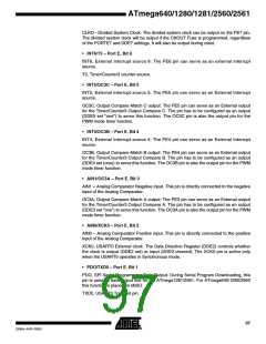
Table 49 and Table 50 relates the alternate functions of Port E to the overriding signals
shown in Figure 37 on page 86.
Table 49. Overriding Signals for Alternate Functions PE7..PE4
Signal
Name
PUOE
PUOV
DDOE
DDOV
PVOE
PVOV
DIEOE
DIEOV
DI
PE7/INT7/ICP3
PE6/INT6/T3
PE5/INT5/OC3C
PE4/INT4/OC3B
0
0
0
0
0
0
0
0
0
0
0
0
0
0
0
0
0
0
OC3C ENABLE
OC3C
OC3B ENABLE
OC3B
0
0
INT7 ENABLE
1
INT6 ENABLE
1
INT5 ENABLE
1
INT4 ENABLE
1
INT7 INPUT/ICP3
INPUT
INT7 INPUT/T3
INPUT
INT5 INPUT
INT4 INPUT
AIO
–
–
–
–
98
ATmega640/1280/1281/2560/2561
2549A–AVR–03/05

 ATMEL [ ATMEL ]