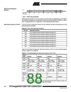
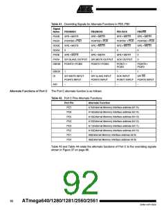
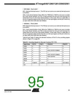
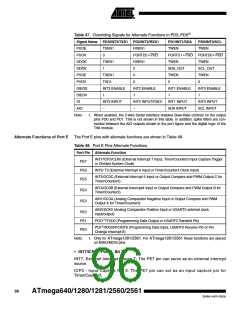
Table 41. Overriding Signals for Alternate Functions in PB3..PB0
Signal
Name
PUOE
PUOV
DDOE
DDOV
PVOE
PVOV
DIEOE
PB3/MISO
SPE • MSTR
PORTB3 • PUD
SPE • MSTR
0
PB2/MOSI
SPE • MSTR
PORTB2 • PUD
SPE • MSTR
0
PB1/SCK
PB0/SS
SPE • MSTR
SPE • MSTR
PORTB1 • PUD PORTB0 • PUD
SPE • MSTR
0
SPE • MSTR
0
0
0
SPE • MSTR
SPE • MSTR
SPE • MSTR
SPI SLAVE OUTPUT SPI MSTR OUTPUT SCK OUTPUT
PCINT3 • PCIE0
PCINT2 • PCIE0
PCINT1 •
PCIE0
PCINT0 •
PCIE0
DIEOV
DI
1
1
1
1
SPI MSTR INPUT
PCINT3 INPUT
SPI SLAVE INPUT
PCINT2 INPUT
SCK INPUT
SPI SS
PCINT1 INPUT
PCINT0 INPUT
AIO
–
–
–
–
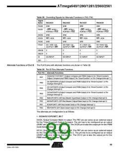
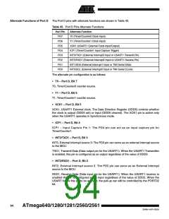
Alternate Functions of Port C The Port C alternate function is as follows:
Table 42. Port C Pins Alternate Functions
Port Pin
PC7
Alternate Function
A15(External Memory interface address bit 15)
A14(External Memory interface address bit 14)
A13(External Memory interface address bit 13)
A12(External Memory interface address bit 12)
A11(External Memory interface address bit 11)
A10(External Memory interface address bit 10)
A9(External Memory interface address bit 9)
A8(External Memory interface address bit 8)
PC6
PC5
PC4
PC3
PC2
PC1
PC0
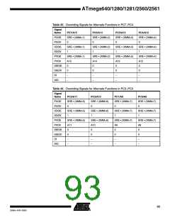
Table 43 and Table 44 relate the alternate functions of Port C to the overriding signals
shown in Figure 37 on page 86.
92
ATmega640/1280/1281/2560/2561
2549A–AVR–03/05

 ATMEL [ ATMEL ]