ATmega640/1280/1281/2560/2561
When the SPI0 is enabled as a master, the data direction of this pin is controlled by
DDB1. When the pin is forced to be an input, the pull-up can still be controlled by the
PORTB1 bit.
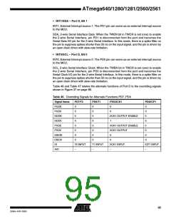
PCINT1, Pin Change Interrupt source 1: The PB7 pin can serve as an external interrupt
source.
• SS/PCINT0 – Port B, Bit 0
SS: Slave Port Select input. When the SPI is enabled as a slave, this pin is configured
as an input regardless of the setting of DDB0. As a slave, the SPI is activated when this
pin is driven low. When the SPI is enabled as a master, the data direction of this pin is
controlled by DDB0. When the pin is forced to be an input, the pull-up can still be con-
trolled by the PORTB0 bit.
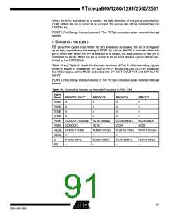
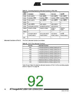
Table 40 and Table 41 relate the alternate functions of Port B to the overriding signals
shown in Figure 37 on page 86. SPI MSTR INPUT and SPI SLAVE OUTPUT constitute
the MISO signal, while MOSI is divided into SPI MSTR OUTPUT and SPI SLAVE
INPUT.
PCINT0, Pin Change Interrupt source 0: The PB7 pin can serve as an external interrupt
source..
Table 40. Overriding Signals for Alternate Functions in PB7..PB4
Signal
Name
PUOE
PUOV
DDOE
DDOV
PVOE
PVOV
DIEOE
DIEOV
DI
PB7/OC0A/OC1C
PB6/OC1B
PB5/OC1A
PB4/OC2
0
0
0
0
0
0
0
0
0
0
0
0
0
0
0
0
OC0/OC1C ENABLE
OC1B ENABLE
OC1A ENABLE
OC2 ENABLE
OC0/OC1C
OC1B
OC1A
OC2B
PCINT7 • PCIE0
PCINT6 • PCIE0
PCINT5 • PCIE0
PCINT4 • PCIE0
1
1
1
1
PCINT7 INPUT
–
PCINT6 INPUT
–
PCINT5 INPUT
–
PCINT4 INPUT
–
AIO
91
2549A–AVR–03/05

 ATMEL [ ATMEL ]