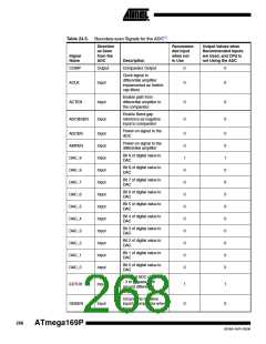
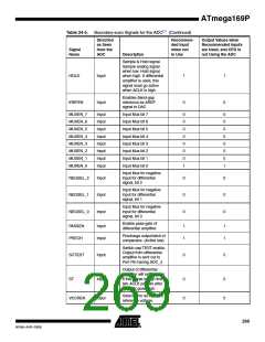
Table 24-5. Boundary-scan Signals for the ADC(1)
Direction
as Seen
from the
ADC
Recommen-
ded Input
when not
in Use
Output Values when
Recommended Inputs
are Used, and CPU is
not Using the ADC
Signal
Name
Description
COMP
Output
Comparator Output
0
0
Clock signal to
differential amplifier
implemented as Switch-
cap filters
ACLK
Input
0
0
Enable path from
differential amplifier to
the comparator
ACTEN
Input
Input
0
0
0
0
Enable Band-gap
reference as negative
input to comparator
ADCBGEN
Power-on signal to the
ADC
ADCEN
AMPEN
DAC_9
DAC_8
DAC_7
DAC_6
DAC_5
DAC_4
DAC_3
DAC_2
DAC_1
DAC_0
Input
Input
Input
Input
Input
Input
Input
Input
Input
Input
Input
Input
0
0
1
0
0
0
0
0
0
0
0
0
0
0
1
0
0
0
0
0
0
0
0
0
Power-on signal to the
differential amplifier
Bit 9 of digital value to
DAC
Bit 8 of digital value to
DAC
Bit 7 of digital value to
DAC
Bit 6 of digital value to
DAC
Bit 5 of digital value to
DAC
Bit 4 of digital value to
DAC
Bit 3 of digital value to
DAC
Bit 2 of digital value to
DAC
Bit 1 of digital value to
DAC
Bit 0 of digital value to
DAC
Connect ADC channels 0
- 3 to by-pass path
around differential
amplifier
EXTCH
GNDEN
Input
Input
1
0
1
0
Ground the negative
input to comparator when
true
268
ATmega169P
8018A–AVR–03/06

 ATMEL [ ATMEL ]