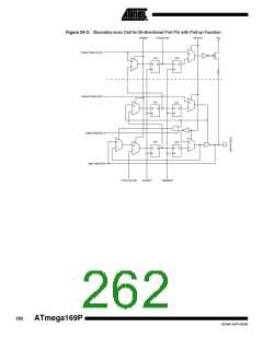
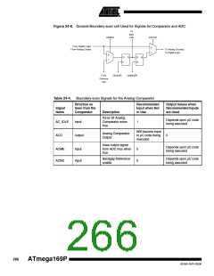
24.5.2
Scanning the RESET Pin
The RESET pin accepts 5V active low logic for standard reset operation, and 12V active high
logic for High Voltage Parallel programming. An observe-only cell as shown in Figure 24-5 is
inserted both for the 5V reset signal; RSTT, and the 12V reset signal; RSTHV.
Figure 24-5. Observe-only Cell
To
Next
ShiftDR
Cell
From System Pin
To System Logic
FF1
0
1
D
Q
From
ClockDR
Previous
Cell
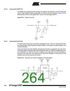
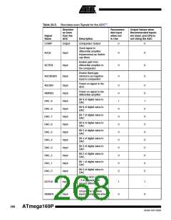
24.5.3
Scanning the Clock Pins
The AVR devices have many clock options selectable by fuses. These are: Internal RC Oscilla-
tor, External Clock, (High Frequency) Crystal Oscillator, Low-frequency Crystal Oscillator, and
Ceramic Resonator.
Figure 24-6 shows how each Oscillator with external connection is supported in the scan chain.
The Enable signal is supported with a general Boundary-scan cell, while the Oscillator/clock out-
put is attached to an observe-only cell. In addition to the main clock, the timer Oscillator is
scanned in the same way. The output from the internal RC Oscillator is not scanned, as this
Oscillator does not have external connections.
Figure 24-6. Boundary-scan Cells for Oscillators and Clock Options
XTAL1/TOSC1
XTAL2/TOSC2
To
Next
Cell
To
ShiftDR
EXTEST
Next
Cell
Oscillator
ShiftDR
From Digital Logic
0
1
To System Logic
ENABLE
OUTPUT
0
1
FF1
D
Q
D
G
Q
0
1
D
Q
From
ClockDR
UpdateDR
Previous
Cell
From
ClockDR
Previous
Cell
264
ATmega169P
8018A–AVR–03/06

 ATMEL [ ATMEL ]