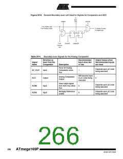
Note:
1. Incorrect setting of the switches in Figure 24-9 will make signal contention and may damage
the part. There are several input choices to the S&H circuitry on the negative input of the out-
put comparator in Figure 24-9. Make sure only one path is selected from either one ADC pin,
Bandgap reference source, or Ground.
If the ADC is not to be used during scan, the recommended input values from Table 24-5 should
be used. The user is recommended not to use the Differential Amplifier during scan. Switch-Cap
based differential amplifier requires fast operation and accurate timing which is difficult to obtain
when used in a scan chain. Details concerning operations of the differential amplifier is therefore
not provided.
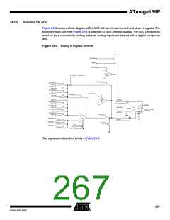
The AVR ADC is based on the analog circuitry shown in Figure 24-9 with a successive approxi-
mation algorithm implemented in the digital logic. When used in Boundary-scan, the problem is
usually to ensure that an applied analog voltage is measured within some limits. This can easily
be done without running a successive approximation algorithm: apply the lower limit on the digi-
tal DAC[9:0] lines, make sure the output from the comparator is low, then apply the upper limit
on the digital DAC[9:0] lines, and verify the output from the comparator to be high.
The ADC need not be used for pure connectivity testing, since all analog inputs are shared with
a digital port pin as well.
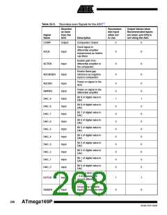
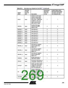
When using the ADC, remember the following
• The port pin for the ADC channel in use must be configured to be an input with pull-up disabled
to avoid signal contention.
• In Normal mode, a dummy conversion (consisting of 10 comparisons) is performed when
enabling the ADC. The user is advised to wait at least 200ns after enabling the ADC before
controlling/observing any ADC signal, or perform a dummy conversion before using the first
result.
• The DAC values must be stable at the midpoint value 0x200 when having the HOLD signal low
(Sample mode).
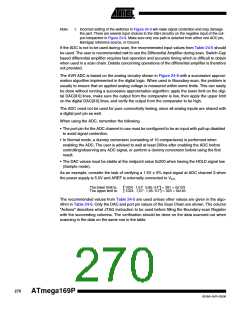
As an example, consider the task of verifying a 1.5V 5ꢀ input signal at ADC channel 3 when
the power supply is 5.0V and AREF is externally connected to VCC
.
The lower limit is:
The upper limit is:
1024 ⋅ 1,5V ⋅ 0,95 ⁄ 5V = 291 = 0x123
1024 ⋅ 1,5V ⋅ 1,05 ⁄ 5V = 323 = 0x143
The recommended values from Table 24-5 are used unless other values are given in the algo-
rithm in Table 24-6. Only the DAC and port pin values of the Scan Chain are shown. The column
“Actions” describes what JTAG instruction to be used before filling the Boundary-scan Register
with the succeeding columns. The verification should be done on the data scanned out when
scanning in the data on the same row in the table.
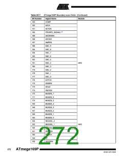
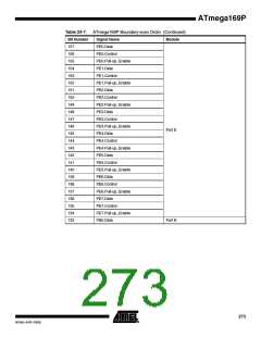
270
ATmega169P
8018A–AVR–03/06

 ATMEL [ ATMEL ]