ATmega169P
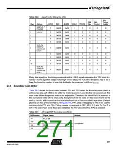
Table 24-6. Algorithm for Using the ADC
PA3.
PA3.
Data
PA3.
Control
Pull-up_
Enable
Step
Actions
ADCEN
DAC
MUXEN
HOLD
PRECH
SAMPLE_P
RELOAD
1
1
0x200
0x08
1
1
0
0
0
2
3
4
5
EXTEST
1
1
1
1
0x200
0x200
0x123
0x123
0x08
0x08
0x08
0x08
0
1
1
1
1
1
1
0
0
0
0
0
0
0
0
0
0
0
0
0
Verify the
COMP bit
scanned out
to be 0
6
1
0x200
0x08
1
1
0
0
0
7
1
1
1
1
0x200
0x200
0x143
0x143
0x08
0x08
0x08
0x08
0
1
1
1
1
1
1
0
0
0
0
0
0
0
0
0
0
0
0
0
8
9
10
Verify the
COMP bit
scanned out
to be 1
11
1
0x200
0x08
1
1
0
0
0
Using this algorithm, the timing constraint on the HOLD signal constrains the TCK clock fre-
quency. As the algorithm keeps HOLD high for five steps, the TCK clock frequency has to be at
least five times the number of scan bits divided by the maximum hold time, thold,max
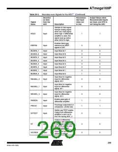
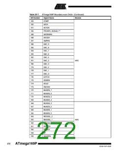
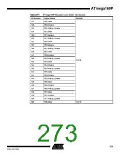
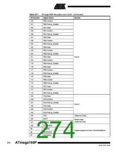
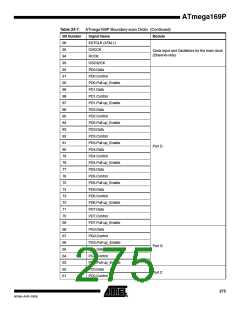
24.6 Boundary-scan Order
Table 24-7 shows the Scan order between TDI and TDO when the Boundary-scan chain is
selected as data path. Bit 0 is the LSB; the first bit scanned in, and the first bit scanned out. The
scan order follows the pin-out order as far as possible. Therefore, the bits of Port A is scanned in
the opposite bit order of the other ports. Exceptions from the rules are the Scan chains for the
analog circuits, which constitute the most significant bits of the scan chain regardless of which
physical pin they are connected to. In Figure 24-3, PXn. Data corresponds to FF0, PXn. Control
corresponds to FF1, and PXn. Pull-up_enable corresponds to FF2. Bit 4, 5, 6, and 7of Port F is
not in the scan chain, since these pins constitute the TAP pins when the JTAG is enabled.
Table 24-7. ATmega169P Boundary-scan Order
Bit Number
197
Signal Name
AC_IDLE
ACO
Module
196
Comparator
195
ACME
194
AINBG
271
8018A–AVR–03/06

 ATMEL [ ATMEL ]