AT90PWM2/3/2B/3B
When this bit is written logic one, the digital input buffer on the corresponding ADC pin is dis-
abled. The corresponding PIN Register bit will always read as zero when this bit is set. When an
analog signal is applied to the ADC7..0 pin and the digital input from this pin is not needed, this
bit should be written logic one to reduce power consumption in the digital input buffer.
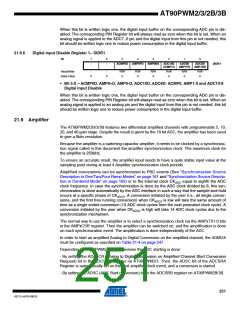
21.8.6
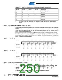
Digital Input Disable Register 1– DIDR1
Bit
7
6
5
4
3
2
1
0
-
-
ACMP0D
AMP0PD AMP0ND
ADC10D
ACMP1D
ADC9D
AMP1PD AMP1ND
ADC8D
DIDR1
Read/Write
Initial Value
-
-
R/W
0
R/W
0
R/W
0
R/W
0
R/W
0
R/W
0
0
0
• Bit 5:0 – ACMP0D, AMP0+D, AMP0-D, ADC10D..ADC8D: ACMP0, AMP1:0 and ADC10:8
Digital Input Disable
When this bit is written logic one, the digital input buffer on the corresponding ADC pin is dis-
abled. The corresponding PIN Register bit will always read as zero when this bit is set. When an
analog signal is applied to an analog pin and the digital input from this pin is not needed, this bit
should be written logic one to reduce power consumption in the digital input buffer.
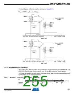
21.9 Amplifier
The AT90PWM2/2B/3/3B features two differential amplified channels with programmable 5, 10,
20, and 40 gain stage. Despite the result is given by the 10 bit ADC, the amplifier has been sized
to give a 8bits resolution.
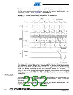
Because the amplifier is a switching capacitor amplifier, it needs to be clocked by a synchroniza-
tion signal called in this document the amplifier synchronization clock. The maximum clock for
the amplifier is 250kHz.
To ensure an accurate result, the amplifier input needs to have a quite stable input value at the
sampling point during at least 4 Amplifier synchronization clock periods.
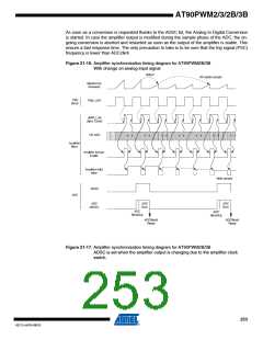
Amplified conversions can be synchronized to PSC events (See “Synchronization Source
Description in One/Two/Four Ramp Modes” on page 161 and “Synchronization Source Descrip-
tion in Centered Mode” on page 162) or to the internal clock CKADC equal to eighth the ADC
clock frequency. In case the synchronization is done by the ADC clock divided by 8, this syn-
chronization is done automatically by the ADC interface in such a way that the sample-and-hold
occurs at a specific phase of CKADC2. A conversion initiated by the user (i.e., all single conver-
sions, and the first free running conversion) when CKADC2 is low will take the same amount of
time as a single ended conversion (13 ADC clock cycles from the next prescaled clock cycle). A
conversion initiated by the user when CKADC2 is high will take 14 ADC clock cycles due to the
synchronization mechanism.
The normal way to use the amplifier is to select a synchronization clock via the AMPxTS1:0 bits
in the AMPxCSR register. Then the amplifier can be switched on, and the amplification is done
on each synchronization event. The amplification is done independently of the ADC.
In order to start an amplified Analog to Digital Conversion on the amplified channel, the ADMUX
must be configured as specified on Table 21-4 on page 247.
Depending on AT90PWM2/2B/3/3B revision the ADC starting is done:
- By setting the ADASCR (Analog to Digital Conversion on Amplified Channel Start Conversion
Request) bit in the ADCSRB register on AT90PWM2/3. Then, the ADSC bit of the ADCSRA
Register is automatically set on the next amplifier clock event, and a conversion is started.
- By setting the ADSC (ADC Start conversion) bit in the ADCSRB register on AT90PWM2B/3B.
251
4317J–AVR–08/10

 ATMEL [ ATMEL ]