AT90PWM2/3/2B/3B
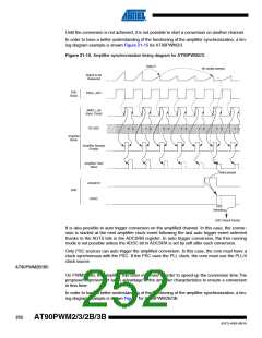
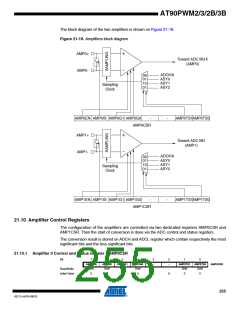
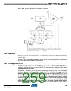
The block diagram of the two amplifiers is shown on Figure 21-18.
Figure 21-18. Amplifiers block diagram
AMP0+
AMP0-
+
-
Toward ADC MUX
(AMP0)
ADCK/8
ASY0
00
01
10
01
ASY1
ASY2
Sampling
Clock
AMP0EN AMP0IS AMP0G1 AMP0G0
-
-
AMP0TS1AMP0TS0
AMP0CSR
AMP1+
AMP1-
+
-
Toward ADC MU
(AMP1)
ADCK/8
ASY0
00
01
10
01
ASY1
ASY2
Sampling
Clock
AMP1EN AMP1IS AMP1G1 AMP1G0
-
-
AMP1TS1AMP1TS0
AMP1CSR
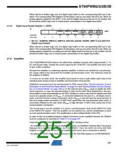
21.10 Amplifier Control Registers
The configuration of the amplifiers are controlled via two dedicated registers AMP0CSR and
AMP1CSR. Then the start of conversion is done via the ADC control and status registers.
The conversion result is stored on ADCH and ADCL register which contain respectively the most
significant bits and the less significant bits.
21.10.1 Amplifier 0 Control and Status register – AMP0CSR
Bit
7
6
5
4
AMP0G0
R/W
0
3
-
2
-
1
AMP0TS1
R/W
0
AMP0TS0
R/W
AMP0EN
AMP0IS
AMP0G1
AMP0CSR
Read/Write
Initial Value
R/W
0
R/W
0
R/W
0
-
-
0
0
0
0
255
4317J–AVR–08/10

 ATMEL [ ATMEL ]