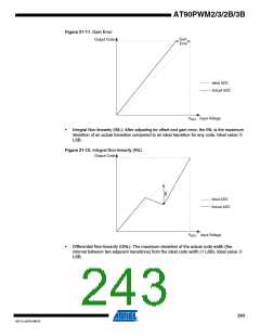
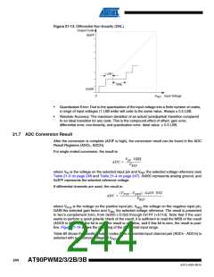
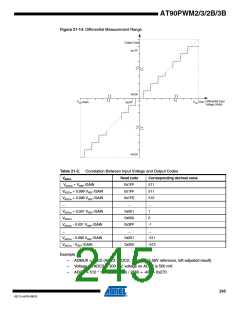
AT90PWM2/3/2B/3B
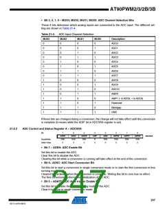
• Bit 3, 2, 1, 0 – MUX3, MUX2, MUX1, MUX0: ADC Channel Selection Bits
These 4 bits determine which analog inputs are connected to the ADC input. The different set-
ting are shown in Table 21-4.
Table 21-4. ADC Input Channel Selection
MUX3
MUX2
MUX1
MUX0
Description
0
0
0
0
0
0
0
0
1
1
1
1
1
1
1
1
0
0
0
0
1
1
1
1
0
0
0
0
1
1
1
1
0
0
1
1
0
0
1
1
0
0
1
1
0
0
1
1
0
1
0
1
0
1
0
1
0
1
0
1
0
1
0
1
ADC0
ADC1
ADC2
ADC3
ADC4
ADC5
ADC6
ADC7
ADC8
ADC9
ADC10
AMP0
AMP1 (- is ADC8, + is ADC9)
Reserved
Bandgap
GND
If these bits are changed during a conversion, the change will not take effect until this conversion
is complete (it means while the ADIF bit in ADCSRA register is set).
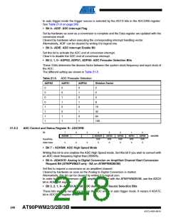
21.8.2
ADC Control and Status Register A – ADCSRA
Bit
7
6
5
4
ADIF
R
3
ADIE
R/W
0
2
ADPS2
R/W
0
1
ADPS1
R/W
0
0
ADPS0
R/W
0
ADEN
ADSC
ADATE
R/W
0
ADCSRA
Read/Write
Initial Value
R/W
0
R/W
0
0
• Bit 7 – ADEN: ADC Enable Bit
Set this bit to enable the ADC.
Clear this bit to disable the ADC.
Clearing this bit while a conversion is running will take effect at the end of the conversion.
• Bit 6– ADSC: ADC Start Conversion Bit
Set this bit to start a conversion in single conversion mode or to start the first conversion in free
running mode.
Cleared by hardware when the conversion is complete. Writing this bit to zero has no effect.
The first conversion performs the initialization of the ADC.
• Bit 5 – ADATE: ADC Auto trigger Enable Bit
Set this bit to enable the auto triggering mode of the ADC.
Clear it to return in single conversion mode.
247
4317J–AVR–08/10

 ATMEL [ ATMEL ]