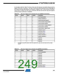
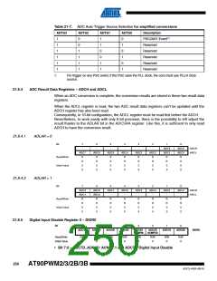
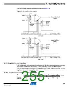
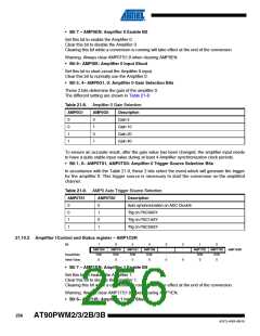
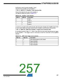
AT90PWM2/3/2B/3B
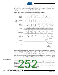
As soon as a conversion is requested thanks to the ADSC bit, the Analog to Digital Conversion
is started. In case the amplifier output is modified during the sample phase of the ADC, the on-
going conversion is aborted and restarted as soon as the output of the amplifier is stable. This
ensure a fast response time. The only precaution to take is to be sure that the trig signal (PSC)
frequency is lower than ADCclk/4.
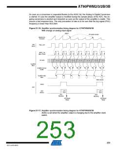
Figure 21-16. Amplifier synchronization timing diagram for AT90PWM2B/3B
With change on analog input signal
DeltaV
4th stable sample
Signalto be
measured
PSC
Block
PSCn_ASY
AMPLI_clk
(Sync Clock)
CK ADC
Valid sample
ADSC
ADC
ADC
Activity
ADC
Conv
ADC
Conv
ADC
Sampling
ADC
Sampling
ADCResult
Ready
ADCResult
Ready
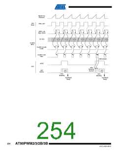
Figure 21-17. Amplifier synchronization timing diagram for AT90PWM2B/3B
ADSC is set when the amplifier output is changing due to the amplifier clock
switch.
253
4317J–AVR–08/10

 ATMEL [ ATMEL ]