AT89C5132
21. Analog to Digital Converter
The AT89C5132 implement a 2-channel 10-bit (8 true bits) analog to digital converter (ADC).
First channel of this ADC can be used for battery monitoring while the second one can be used
for voice sampling at 8 kHz.
21.1 Description
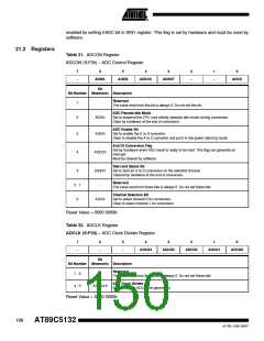
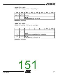
The A/D converter interfaces with the C51 core through four special function registers: ADCON,
the ADC control register (see Table 31); ADDH and ADDL, the ADC data registers (see Table 33
and Table 34); and ADCLK, the ADC clock register (see Table 32).
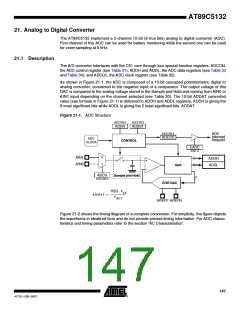
As shown in Figure 21-1, the ADC is composed of a 10-bit cascaded potentiometric digital to
analog converter, connected to the negative input of a comparator. The output voltage of this
DAC is compared to the analog voltage stored in the Sample and Hold and coming from AIN0 or
AIN1 input depending on the channel selected (see Table 30). The 10-bit ADDAT converted
value (see formula in Figure 21-1) is delivered in ADDH and ADDL registers, ADDH is giving the
8 most significant bits while ADDL is giving the 2 least significant bits. ADDAT
Figure 21-1. ADC Structure
ADCON.5
ADCON.3
ADEN
ADSST
ADCON.4
ADC
Interrupt
Request
ADEOC
ADC
CLOCK
CONTROL
EADC
IEN1.3
8
2
0
1
AIN1
AIN0
ADDH
ADDL
+
-
SAR
AVSS
ADCS
ADCON.0
Sample and Hold
10
R/2R DAC
1023 ⋅ V
--------------------------
IN
ADDAT =
V
REF
AREFP AREFN
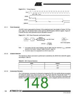
Figure 21-2 shows the timing diagram of a complete conversion. For simplicity, the figure depicts
the waveforms in idealized form and do not provide precise timing information. For ADC charac-
teristics and timing parameters refer to the section “AC Characteristics”.
147
4173E–USB–09/07

 ATMEL [ ATMEL ]