18.4.2
18.4.3
Reception
(Modes 1, 2 and 3)
To prepare for reception, write to SCON register, setting SM0 and SM1 Bits according to
Table 89, and set the REN bit. The actual reception is then initiated by a detected high-to-low
transition on the RXD pin.
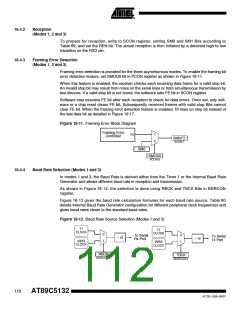
Framing Error Detection
(Modes 1, 2 and 3)
Framing error detection is provided for the three asynchronous modes. To enable the framing bit
error detection feature, set SMOD0 bit in PCON register as shown in Figure 18-11.
When this feature is enabled, the receiver checks each incoming data frame for a valid stop bit.
An invalid stop bit may result from noise on the serial lines or from simultaneous transmission by
two devices. If a valid stop bit is not found, the software sets FE bit in SCON register.
Software may examine FE bit after each reception to check for data errors. Once set, only soft-
ware or a chip reset clears FE bit. Subsequently received frames with valid stop Bits cannot
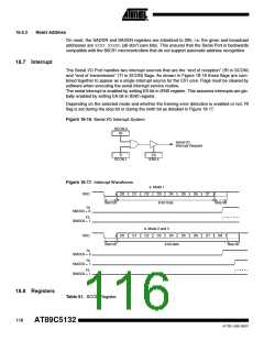
clear FE bit. When the framing error detection feature is enabled, RI rises on stop bit instead of
the last data bit as detailed in Figure 18-17.
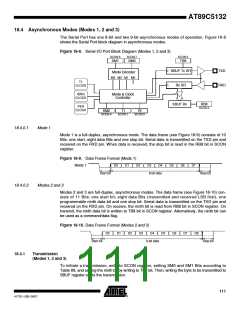
Figure 18-11. Framing Error Block Diagram
Framing Error
Controller
FE
1
0
SM0/FE
SCON.7
SM0
SMOD0
PCON.6
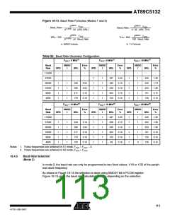
18.4.4
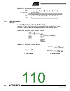
Baud Rate Selection (Modes 1 and 3)
In modes 1 and 3, the Baud Rate is derived either from the Timer 1 or the Internal Baud Rate
Generator and allows different baud rate in reception and transmission.
As shown in Figure 18-12, the selection is done using RBCK and TBCK Bits in BDRCON
register.
Figure 18-13 gives the baud rate calculation formulas for each baud rate source. Table 90
details Internal Baud Rate Generator configuration for different peripheral clock frequencies and
gives baud rates closer to the standard baud rates.
Figure 18-12. Baud Rate Source Selection (Modes 1 and 3)
T1
T1
CLOCK
CLOCK
0
0
1
To Serial
Rx Port
To Serial
Tx Port
÷ 16
÷ 16
1
IBRG
CLOCK
IBRG
CLOCK
RBCK
BDRCON.2
TBCK
BDRCON.3
112
AT89C5132
4173E–USB–09/07

 ATMEL [ ATMEL ]