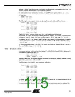
AT89C5132
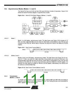
18.4 Asynchronous Modes (Modes 1, 2 and 3)
The Serial Port has one 8-bit and two 9-bit asynchronous modes of operation. Figure 18-8
shows the Serial Port block diagram in asynchronous modes.
Figure 18-8. Serial I/O Port Block Diagram (Modes 1, 2 and 3)
SCON.6
SCON.7
SCON.3
SM1
SM0
TB8
SBUF Tx SR
Rx SR
TXD
RXD
Mode Decoder
M3 M2 M1 M0
T1
CLOCK
IBRG
CLOCK
Mode & Clock
Controller
SBUF Rx
RB8
SCON.2
PER
CLOCK
SM2
SCON.4
TI
SCON.1
RI
SCON.0
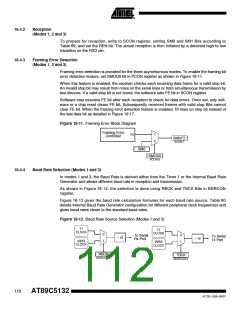
18.4.0.1
Mode 1
Mode 1 is a full-duplex, asynchronous mode. The data frame (see Figure 18-9) consists of 10
Bits: one start, eight data Bits and one stop bit. Serial data is transmitted on the TXD pin and
received on the RXD pin. When data is received, the stop bit is read in the RB8 bit in SCON
register.
Figure 18-9. Data Frame Format (Mode 1)
Mode 1
D0
D1
D2
D3
D4
D5
D6
D7
Start bit
8-bit data
Stop bit
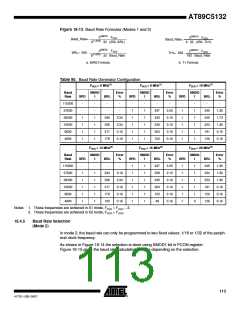
18.4.0.2
Modes 2 and 3
Modes 2 and 3 are full-duplex, asynchronous modes. The data frame (see Figure 18-10) con-
sists of 11 Bits: one start bit, eight data Bits (transmitted and received LSB first), one
programmable ninth data bit and one stop bit. Serial data is transmitted on the TXD pin and
received on the RXD pin. On receive, the ninth bit is read from RB8 bit in SCON register. On
transmit, the ninth data bit is written to TB8 bit in SCON register. Alternatively, the ninth bit can
be used as a command/data flag.
Figure 18-10. Data Frame Format (Modes 2 and 3)
D0
D1
D2
D3
D4
D5
D6
D7
D8
Start bit
9-bit data
Stop bit
18.4.1
Transmission
(Modes 1, 2 and 3)
To initiate a transmission, write to SCON register, setting SM0 and SM1 Bits according to
Table 89, and setting the ninth bit by writing to TB8 bit. Then, writing the byte to be transmitted to
SBUF register starts the transmission.
111
4173E–USB–09/07

 ATMEL [ ATMEL ]