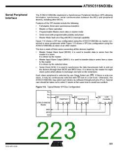
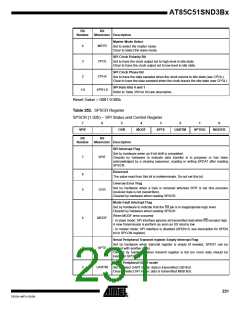
AT85C51SND3Bx
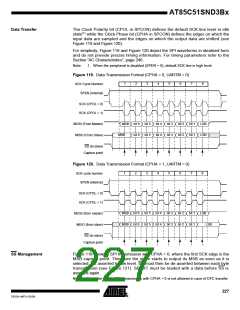
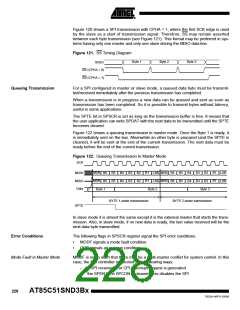
Data Transfer
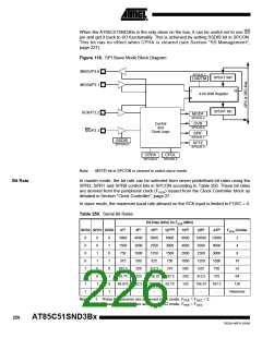
The Clock Polarity bit (CPOL in SPCON) defines the default SCK line level in idle
state(1) while the Clock Phase bit (CPHA in SPCON) defines the edges on which the
input data are sampled and the edges on which the output data are shifted (see
Figure 119 and Figure 120).
For simplicity, Figure 119 and Figure 120 depict the SPI waveforms in idealized form
and do not provide precise timing information. For timing parameters refer to the
Section “AC Characteristics”, page 246.
Note:
1. When the peripheral is disabled (SPEN = 0), default SCK line is high level.
Figure 119. Data Transmission Format (CPHA = 0, UARTM = 0)
1
2
3
4
5
6
7
8
SCK Cycle Number
SPEN (Internal)
SCK (CPOL = 0)
SCK (CPOL = 1)
MSB bit 6
bit 5
bit 5
bit 4
bit 4
bit 3
bit 3
bit 2
bit 2
bit 1
bit 1
LSB
LSB
MOSI (From Master)
MISO (From Slave)
MSB
bit 6
SS (to slave)
Capture point
Figure 120. Data Transmission Format (CPHA = 1, UARTM = 0)
1
2
3
4
5
6
7
8
SCK cycle number
SPEN (internal)
SCK (CPOL = 0)
SCK (CPOL = 1)
MSB bit 6
MSB bit 6
bit 5
bit 5
bit 4
bit 4
bit 3
bit 3
bit 2
bit 2
bit 1
bit 1
LSB
MOSI (from master)
MISO (from slave)
LSB
SS (to slave)
Capture point
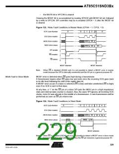
SS Management
Figure 119 shows a SPI transmission with CPHA = 0, where the first SCK edge is the
MSB capture point. Therefore the slave starts to output its MSB as soon as it is
selected: SS asserted to low level. SS must then be de-asserted between each byte
transmission (see Figure 121). SPDAT must be loaded with a data before SS is
asserted again.
Note:
In master mode, SPI transmission with CPHA = 0 is not allowed in case of DFC transfer.
227
7632A–MP3–03/06

 ATMEL [ ATMEL ]