AT85C51SND3Bx
Serial Peripheral
Interface
The AT85C51SND3Bx implement a Synchronous Peripheral Interface (SPI) allowing
full-duplex, synchronous, serial communication between the MCU and peripheral
devices, including other MCUs.
Features of the SPI module include the following:
•
•
•
•
•
Full-duplex, three-wire synchronous transfers
Master or Slave operation
Programmable Master clock rates in master mode
Serial clock with programmable polarity and phase
Master Mode fault error flag with MCU interrupt capability
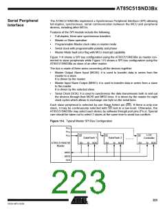
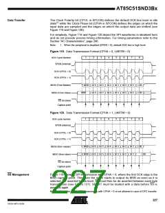
Figure 114 shows a SPI bus configuration using the AT85C51SND3Bx as master con-
nected to slave peripherals while Figure 115 shows a SPI bus configuration using the
AT85C51SND3Bx as slave of an other master.
The bus is made of three wires connecting all the devices together:
•
•
•
Master Output Slave Input (MOSI): it is used to transfer data in series from the
master to a slave.
It is driven by the master.
Master Input Slave Output (MISO): it is used to transfer data in series from a slave
to the master.
It is driven by the selected slave.
Serial Clock (SCK): it is used to synchronize the data transmission both in and out
the devices through their MOSI and MISO lines. It is driven by the master for eight
clock cycles which allows to exchange one byte on the serial lines.
Each slave peripheral is selected by one Slave Select pin (SS). If there is only one
slave, it may be continuously selected with SS tied to a low level. Otherwise, the
AT85C51SND3Bx may select each device by software through port pins (Pn.x). Special
care should be taken not to select 2 slaves at the same time to avoid bus conflicts.
Figure 114. Typical Master SPI Bus Configuration
Pn.z
Pn.y
LCD
Controller
Pn.x
SS
SS
SS
SO
DataFlash 1
SI SCK
DataFlash 2
SO
SO SI SCK
SI SCK
AT85C51SND3B
Master
MISO
MOSI
SCK
223
7632A–MP3–03/06

 ATMEL [ ATMEL ]