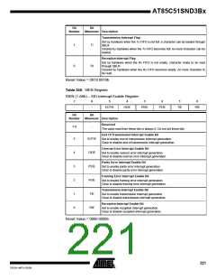
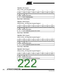
AT85C51SND3Bx
The transmission begins by writing to SPDAT through CPU or DFC. Writing to SPDAT
writes to an intermediate register which is automatically loaded to the shift register if no
transmission is in progress. Reading SPDAT through CPU or DFC reads an intermedi-
ate register updated at the end of each transfer.
The byte begins shifting out on the MOSI pin under the control of the bit rate generator.
This generator also controls the shift register of the slave peripheral through the SCK
output pin. As the byte shifts out, another byte shifts in from the slave peripheral on the
MISO pin. The byte is transmitted most significant bit (MSB) first when UARTM bit in
SPCR is cleared or least significant bit (LSB) first when UARTM bit in SPCR is set. The
end of transfer is signaled by SPIF being set.
In case SPI is the source of a DFC channel (slave device data read), SPDAT is first
loaded with a dummy byte (FFh value) to initiate the transfer. Then transfer continues by
transmitting the shift register content which is the last data received.
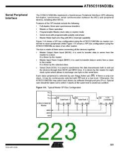
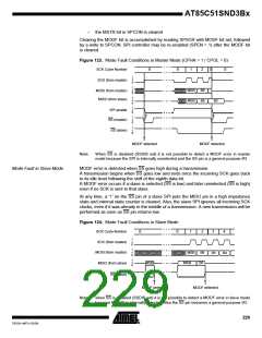
When the AT85C51SND3Bx is the only master on the bus, it can be useful not to use
SS pin and get it back to I/O functionality. This is achieved by setting SSDIS bit in
SPCON.
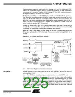
Figure 117. SPI Master Mode Block Diagram
MOSI/P3.1
SPSCR.2
SPDAT WR
UARTM
MISO/P3.0
I
Q
8-bit Shift Register
SPDAT RD
SCK/P3.2
SS/P3.3
MODF
SPSCR.4
SSDIS
SPCON.5
OVR
SPSCR.6
Control
and
Clock Logic
PER
CLOCK
SPIF
SPSCR.7
Bit Rate
Generator
SPTE
SPSCR.3
SPEN
SPCON.6
SPR2:0
SPCON
CPHA
SPCON.2
CPOL
SPCON.3
Note:
MSTR bit in SPCON is set to select master mode.
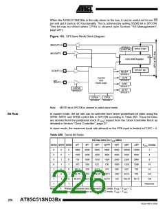
Slave Mode
The SPI operates in slave mode when the MSTR bit in SPCON is cleared and data has
been loaded in SPDAT.
Note:
The SPI Module should be configured as a slave before it is enabled (SPEN set).
Figure 118 shows the SPI block diagram in slave mode. In slave mode, before a data
transmission occurs, the SS pin of the slave SPI must be asserted to low level. SS must
remain low until the transmission of the byte is complete. In the slave SPI module, data
enters the shift register through the MOSI pin under the control of the serial clock pro-
vided by the master SPI module on the SCK input pin. When the master starts a
transmission, the data in the shift register begins shifting out on the MISO pin. The end
of transfer is signaled by SPIF being set.
225
7632A–MP3–03/06

 ATMEL [ ATMEL ]