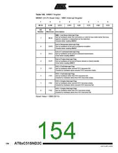
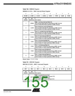
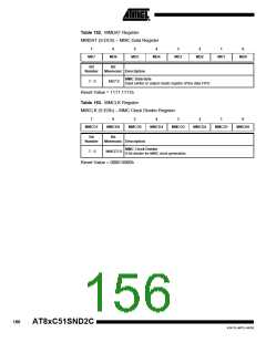
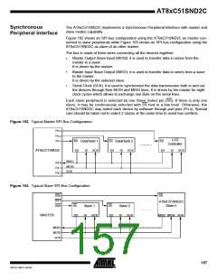
Description
The SPI controller interfaces with the C51 core through three special function registers:
SPCON, the SPI control register (see Table 155); SPSTA, the SPI status register (see
Table 156); and SPDAT, the SPI data register (see Table 157).
Master Mode
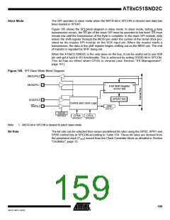
The SPI operates in master mode when the MSTR bit in SPCON is set.
Figure 104 shows the SPI block diagram in master mode. Only a master SPI module
can initiate transmissions. Software begins the transmission by writing to SPDAT. Writ-
ing to SPDAT writes to the shift register while reading SPDAT reads an intermediate
register updated at the end of each transfer.
The Byte begins shifting out on the MOSI pin under the control of the bit rate generator.
This generator also controls the shift register of the slave peripheral through the SCK
output pin. As the Byte shifts out, another Byte shifts in from the slave peripheral on the
MISO pin. The Byte is transmitted most significant bit (MSB) first. The end of transfer is
signaled by SPIF being set.
When the AT8xC51SND2C is the only master on the bus, it can be useful not to use
SS# pin and get it back to I/O functionality. This is achieved by setting SSDIS bit in
SPCON.
Figure 104. SPI Master Mode Block Diagram
MOSI/P4.1
I
Q
MISO/P4.0
SCK/P4.2
SS#/P4.3
8-bit Shift Register
SPDAT WR
SPDAT RD
MODF
SSDIS
SPCON.5
SPSTA.4
Control and Clock Logic
WCOL
SPSTA.6
PER
Bit Rate Generator
CLOCK
SPIF
SPSTA.7
SPEN
SPCON.6
SPR2:0
SPCON
CPHA
SPCON.2
CPOL
SPCON.3
Note:
MSTR bit in SPCON is set to select master mode.
158
AT8xC51SND2C
4341D–MP3–04/05

 ATMEL [ ATMEL ]