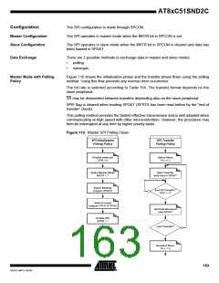
AT8xC51SND2C
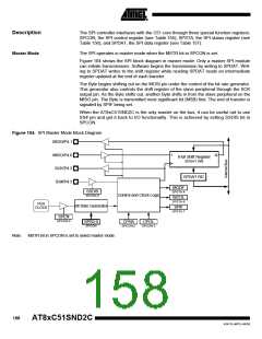
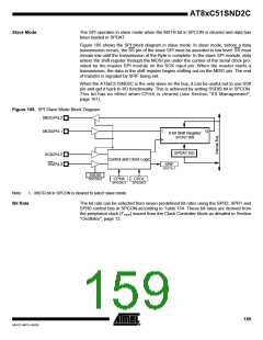
Slave Mode
The SPI operates in slave mode when the MSTR bit in SPCON is cleared and data has
been loaded in SPDAT.
Figure 105 shows the SPI block diagram in slave mode. In slave mode, before a data
transmission occurs, the SS pin of the slave SPI must be asserted to low level. SS must
remain low until the transmission of the Byte is complete. In the slave SPI module, data
enters the shift register through the MOSI pin under the control of the serial clock pro-
vided by the master SPI module on the SCK input pin. When the master starts a
transmission, the data in the shift register begins shifting out on the MISO pin. The end
of transfer is signaled by SPIF being set.
When the AT8xC51SND2C is the only slave on the bus, it can be useful not to use SS#
pin and get it back to I/O functionality. This is achieved by setting SSDIS bit in SPCON.
This bit has no effect when CPHA is cleared (see Section "SS Management",
page 161).
Figure 105. SPI Slave Mode Block Diagram
MISO/P4.2
I
Q
MOSI/P4.1
8-bit Shift Register
SPDAT WR
SPDAT RD
SCK/P4.2
SS/P4.3
Control and Clock Logic
SPIF
SPSTA.7
SSDIS
SPCON.5
CPHA
SPCON.2
CPOL
SPCON.3
Note:
1. MSTR bit in SPCON is cleared to select slave mode.
Bit Rate
The bit rate can be selected from seven predefined bit rates using the SPR2, SPR1 and
SPR0 control bits in SPCON according to Table 154. These bit rates are derived from
the peripheral clock (FPER) issued from the Clock Controller block as detailed in Section
"Oscillator", page 12.
159
4341D–MP3–04/05

 ATMEL [ ATMEL ]