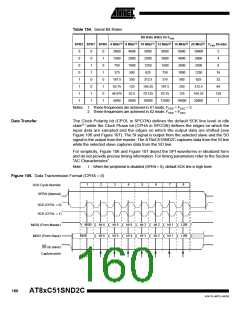
Table 154. Serial Bit Rates
Bit Rate (kHz) Vs FPER
SPR2 SPR1 SPR0 6 MHz(1) 8 MHz(1) 10 MHz(1) 12 MHz(2) 16 MHz(2) 20 MHz(2) FPER Divider
0
0
0
0
1
1
1
1
0
0
1
1
0
0
1
1
0
1
0
1
0
1
0
1
3000
1500
750
4000
2000
1000
500
5000
2500
6000
3000
1500
750
8000
4000
2000
1000
500
10000
5000
2
4
1250
2500
8
375
625
1250
16
32
64
128
1
187.5
93.75
46.875
6000
250
312.5
156.25
78.125
10000
375
625
125
187.5
93.75
12000
250
312.5
156.25
20000
62.5
8000
125
16000
Notes: 1. These frequencies are achieved in X1 mode, FPER = FOSC ÷ 2.
2. These frequencies are achieved in X2 mode, FPER = FOSC
.
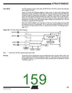
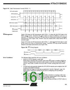
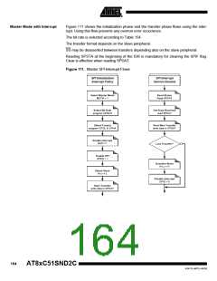
Data Transfer
The Clock Polarity bit (CPOL in SPCON) defines the default SCK line level in idle
state(1) while the Clock Phase bit (CPHA in SPCON) defines the edges on which the
input data are sampled and the edges on which the output data are shifted (see
Figure 106 and Figure 107). The SI signal is output from the selected slave and the SO
signal is the output from the master. The AT8xC51SND2C captures data from the SI line
while the selected slave captures data from the SO line.
For simplicity, Figure 106 and Figure 107 depict the SPI waveforms in idealized form
and do not provide precise timing information. For timing parameters refer to the Section
“AC Characteristics”.
Note:
1. When the peripheral is disabled (SPEN = 0), default SCK line is high level.
Figure 106. Data Transmission Format (CPHA = 0)
1
2
3
4
5
6
7
8
SCK Cycle Number
SPEN (Internal)
SCK (CPOL = 0)
SCK (CPOL = 1)
MSB
bit 6
bit 6
bit 5
bit 5
bit 4
bit 4
bit 3
bit 3
bit 2
bit 2
bit 1
bit 1
LSB
LSB
MOSI (From Master)
MISO (From Slave)
MSB
SS (to slave)
Capture point
160
AT8xC51SND2C
4341D–MP3–04/05

 ATMEL [ ATMEL ]