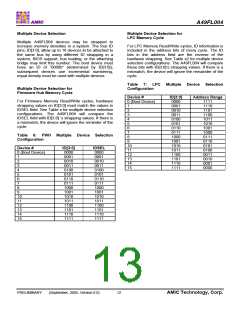
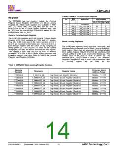
A49FL004
through four consecutive memory write cycles. In A/A Mux
mode, a program operation is activated by writing the three-
byte command sequence and program address/data through
four consecutive bus cycles.
protected. Any attempt to erase or program a sector or block
within this area will be ignored.
Both TBL and WP pins must be set low (VIL) for protection
or high (VIH) for un-protection prior to a program or erase
The row address (A10 - A0) is latched on the falling edge of
R/C and the column address (A21 - A11) is latched on the
rising edge of R/C . The data is latched on the rising edge
operation. A logic level change on TBL or WP pin during a
program or erase operation may cause unpredictable results.
The TBL and WP pins work in combination with the block
locking registers. When active, these pins write protect the
appropriate blocks regardless of the associated block locking
registers setting.
of WE . Once the program operation is started, the internal
control logic automatically handles the internal programming
voltages and timing.
A data “0” can not be programmed back to a “1”. Only erase
Hardware Data Protection
operation can convert “0”s to “1”s. The Data Polling on I/O7
or Toggle Bit on I/O6 can be used to detect when the
programming operation is completed in FWH, LPC, and A/A
Mux modes.
Hardware data protection protects the devices from
unintentional erase or program operation. It is performed by
the device automatically in the following three ways:
(a) VDD Detection: if VDD is below 1.8 V (typical), the program
and erase functions are inhibited.
Data Polling (I/O7)
(b) Write Inhibit Mode: holding any of the signal OE low, or
WE high inhibits a write cycle (A/A Mux mode only).
The device provides a Data Polling feature to indicate the
progress or the completion of a program or erase operation
in all modes. During a program operation, an attempt to read
the device will result in the complement of the last loaded
data on I/O7. Once the program cycle is complete, the true
data of the last loaded data is valid on all outputs. During an
erase operation, an attempt to read the device will result a
“0” on I/O7. After the erase cycle is complete, an attempt to
read the device will result a “1” on I/O7.
(c) Noise/Glitch Protection: pulses of less than 5 ns (typical)
on the WE input will not initiate a write cycle (A/A Mux mode
only).
Reset
Any read, program, or erase operation to the devices can be
reset by the INIT or RST pins. INIT and RST pins are
internally hard-wired and have same function to the devices.
Toggle Bit (I/O6)
The A49FL004 also provides a Toggle Bit feature to detect
the progress or the completion of a program or erase
operation. During a program or erase operation, an attempt
to read data from the devices will result in I/O6 toggling
between “1” and “0”. When the program or erase operation is
complete, I/O6 will stop toggling and valid data will be read.
Toggle bit may be accessed at any time during a program or
erase operation.
The INIT pin is only available in FWH and LPC modes. The
RST pin is available in all modes. It is required to drive
INIT or RST pins low during system reset to ensure proper
initialization.
During a memory read operation, pulls low the INIT or RST
pin will reset the devices back to standby mode and then the
FWH[3:0] of FWH interface or the LAD[3:0] of LPC interface
will go to high impedance state. During a program or erase
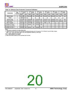
Data Protection
The device features a software data protection function to
protect the device from an unintentional erase or program
operation. It is performed by JEDEC standard Software Data
Protection (SDP) command sequences. See Table 14 for
SDP Command Definition. A program operation is initiated by
three memory write cycles of unlock command sequence.
A chip (only available in A/A Mux mode), sector or block
erase operation is initiated by six memory write cycles of
unlock command sequence. During SDP command
sequence, any invalid command or sequence will abort the
operation and force the device back to standby mode.
operation, pulls low the INIT or RST pin will abort the
program or erase operation and reset the devices back to
standby mode. A reset latency will occur before the devices
resume to standby mode when such reset is performed.
When a program or erase operation is reset before the
completion of such operation, the memory contents of
devices may become invalid due to an incomplete program
or erase operation.
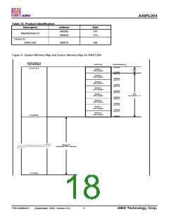
Product Identification
The product identification mode can be used to read the
Manufacturer ID and the Device ID by a software Product ID
Entry command in both in-system hardware interface and
A/A Mux interface modes. The product identification mode is
activated by three-bus-cycle command. Refer to Table 12 for
the Manufacturer ID and Device ID of A49FL004 and Table
14 for the SDP Command Definition.
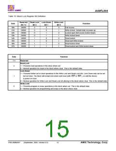
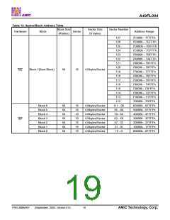
Memory Hardware Write Protection
The A49FL004 has a 64 KByte top boot block. When working
in-system, the memory hardware write protection feature can
be activated by two control pins - Top Block Lock ( TBL ) and
Write Protection ( WP ) for both FWH and LPC modes. When
In FWH mode, the product identification can also be read
directly at FFBC0000h for Manufacturer ID - “99h” and
FFBC0001h for Device ID in the 4 GByte system memory
map.
TBL is pulled low (VIL), the boot block is hardware write
protected. A sector erase, block erase, or byte program
command attempts to erase or program the boot block will be
ignored. When WP is pulled low (VIL), the Block 0 ~ Block 6
of A49FL004 (except the boot block) are hardware write
PRELIMINARY
(September, 2005, Version 0.0)
16
AMIC Technology, Corp.

 AMICC [ AMIC TECHNOLOGY ]