A49FL004
ADDRESS/ADDRESS MULTIPLEXED (A/A
MUX) MODE
The 11 multiplex address pins - A[10:0] and a R/C pin are
used to load the row and column addresses for the target
memory location. The row addresses (internal address A10 -
Read/Write Operation
The A49FL004 offers a Address/Address Multiplexed (A/A
Mux) mode for off-system operation, typically on an EPROM
Programmer, similar to a traditional Flash memory except the
address input is multiplexed. In the A/A Mux mode, the
A0) are latched on the falling edge of R/C pin. The column
addresses (internal address A21 - A11) are latched on the
programmer must drive the OE pin to low (VIL) for read or
WE pins to low for write operation. The devices have no
Chip Enable ( CE ) pin for chip selection and activation as
rising edge of R/C pin. The A49FL004 use A18 - A0
respectively.
During a read operation, the OE signal is used to control the
output of data to the 8 I/O pins - I/O[7:0]. During a write
traditional Flash memory. The R/C , OE and WE pins are
used to activate the device and control the power.
operation, the WE signal is used to latch the input data from
I/O[7:0]. See Table 11 for Bus Operation Modes.
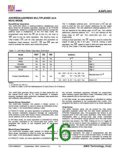
Table 11: A/A Mux Mode Operation Selection
Mode
RST
OE
WE
Address
I/O
Read
Write
VIH
VIH
VIH
VIH
VIL
VIL
VIH
VIH
VIH
X
VIH
VIL
VIH
X
X (1)
X
DOUT
DIN
Standby
Output Disable
Reset
X
High Z
High Z
High Z
X
X
X
A2 – A21 = X, A1 = VIL, A0 = VIL
,
Manufacturer ID (2)
Device ID
and
A1 = VIH, A0 = VIH
Product Identification
VIH
VIL
VIH
A2 – A21= X, A1 = VIL, A0 = VIH
Notes:
1. X can be VIL OR VIH.
2. Refer to Table 12 for the Manufacturer ID and Device ID of devices.
The A49FL004 provides three levels of data protection for
the critical BIOS code of PC and Notebook. It includes
memory hardware write protection, hardware data protection
and software data protection.
the six-byte command sequence through six consecutive
write memory cycles with Block Erase Command (50h), and
Block address (BA) in the last bus cycle.
In A/A Mux mode, an erase operation is activated by writing
the six-byte command in six consecutive bus cycles. Pre-
programs the block is not required prior to an erase operation.
Sector-Erase Operation
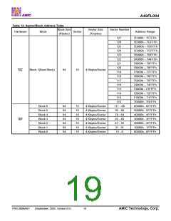
The A49FL004 contains 128 uniform 4 KByte sectors. A
sector erase command is used to erase an individual sector.
See Table 11 for Sector/Block Address Table.
Chip-Erase
The entire memory array can be erased by chip erase
operation available under the A/A Mux mode operated by
EPROM Programmer only. Pre-programs the device is not
required prior to the chip erase operation. Chip erase starts
immediately after a six-bus-cycle chip erase command
sequence. All commands will be ignored once the chip erase
In FWH/LPC mode, an erase operation is activated by writing
the six-byte command sequence through six consecutive
write memory cycles with Sector Erase Command (30h), and
sector address (SA) in the last bus cycle.
In A/A Mux mode, an erase operation is activated by writing
the six-byte command in six consecutive bus cycles. Pre-
programs the sector is not required prior to an erase
operation.
operation has started. The Data Polling on I/O7 or Toggle Bit
on I/O6 can be used to detect the progress or completion of
erase operation. The device will return back to standby mode
after the completion of the chip erase.
Block-Erase Operation
Write Operation Status Detection
The A49FL004 contains eight uniform 64 KByte blocks. A
block erase command is used to erase an individual block.
See Table 13 for Sector/Block Address Table.
In program operation, the data is programmed into the
devices (to a logical “0”) on a byte-by-byte basis. In FWH and
LPC mode, a program operation is activated by writing the
three-byte command sequence and program address/data
In FWH/LPC mode, an erase operation is activated by writing
PRELIMINARY
(September, 2005, Version 0.0)
15
AMIC Technology, Corp.

 AMICC [ AMIC TECHNOLOGY ]