A49FL004
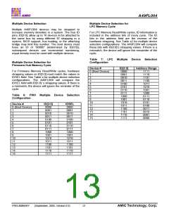
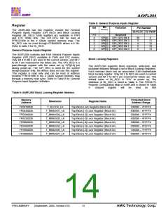
Table 8: General Purpose Inputs Register
Register
Bit
Bit
Function
Pin Number
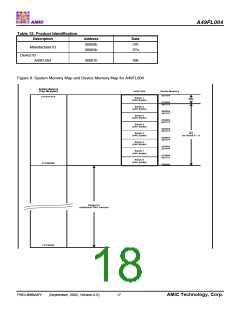
The A49FL004 has two registers include the General
Purpose Inputs Register (GPI_REG) and Block Locking
Register (BL_REG). Both registers are available in FWH
and LPC mode only. The GPI_REG can be read at
FFBC0100h in the 4 GByte system memory map. The
BL_REG can be read through FFBx0002h where x=F-0h.
Refer to table 9 for BL_REG.
32-PLCC 32-TSOP
7:5
4
3
2
1
-
Reserved
-
30
3
4
5
-
6
11
12
13
14
GPI[4]
GPI[3]
GPI[2]
GPI[1]
GPI[0]
GPI_REG Bit 4
GPI_REG Bit 3
GPI_REG Bit 2
GPI_REG Bit 1
GPI_REG Bit 0
0
6
General Purpose Inputs Register
The A49FL004 contains and 8-bit General Purpose Inputs
Register (GPI_REG) available in FWH and LPC modes.
Only Bit 4 to Bit 0 are used in the current version, and bit 7
to bit 5 are reserved for the future use. The GPI_REG is a
pass-through register with the value set by GPI[4:0] pin
during power-up. The GPI_REG is used for the system
design purpose only, the device does not use this register.
This register is read only and can be read at address
location FFBC0100h in the 4 Gbyte system memory map
through a memory read cycle. Refer to Table 8 for General
Purpose Input Register Definition.
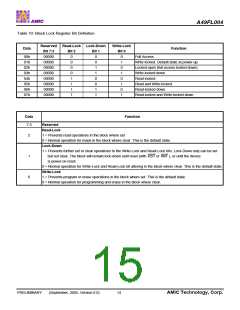
Block Locking Registers
The A49FL004 supports block read-lock, write-lock, and
lockdown features through a set of Block Locking Registers.
Each memory block has an associated 8-bit read/writable
block locking register. Only Bit 2 to Bit 0 are used in current
version and Bit 7 to Bit 3 are reserved for future use. The
default value of BL_REG is “01h” at power up. The
definition of BL_REG is listed in Table 8. The FWH/LPC
Register Configuration Map of A49FL004 is shown in Table
9.
Unused
register
will
be
read
as
00h
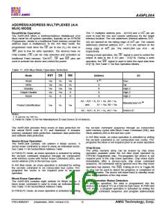
Table 9: A49FL004 Block Locking Register Address
Memory
Mnemonic
Address
Protected Block
Address Range
Register Name
FFBF0002h
FFBE0002h
FFBD0002h
FFBC0002h
FFBB0002h
FFBA0002h
FFB90002h
FFB80002h
T_BLOCK_LK
T_MINUS01_LK
T_MINUS02_LK
T_MINUS03_LK
T_MINUS04_LK
T_MINUS05_LK
T_MINUS06_LK
T_MINUS07_LK
Top Block Lock Register (Block 64)
Top Block [-1] Lock Register (Block 64)
Top Block [-2] Lock Register (Block 64)
Top Block [-3] Lock Register (Block 64)
Top Block [-4] Lock Register (Block 64)
Top Block [-5] Lock Register (Block 64)
Top Block [-6] Lock Register (Block 64)
Top Block [-7] Lock Register (Block 64)
70000h – 7FFFFh
60000h – 6FFFFh
50000h – 5FFFFh
40000h – 4FFFFh
30000h – 3FFFFh
20000h – 2FFFFh
10000h – 1FFFFh
00000h – 0FFFFh
PRELIMINARY
(September, 2005, Version 0.0)
13
AMIC Technology, Corp.

 AMICC [ AMIC TECHNOLOGY ]