A49FL004
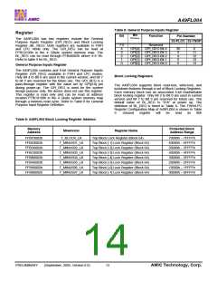
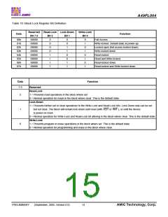
Table 10: Block Lock Register Bit Definition
Reserved
Bit 7:3
Read-Lock Lock-Down
Write-Lock
Bit 0
Data
Function
Bit 2
Bit 1
00h
01h
02h
03h
04h
05h
06h
07h
00000
00000
00000
00000
00000
00000
00000
00000
0
0
0
0
1
1
1
1
0
0
1
1
0
0
1
1
0
1
0
1
0
1
0
1
Full Access.
Write locked. Default state at power-up.
Locked open (full access locked down).
Write-locked down.
Read locked.
Read and Write locked.
Read-locked down
Read-locked and Write-locked down
Data
Function
7:3
2
Reserved
Read-Lock
1 = Prevents read operations in the block where set
0 = Normal operation for reads in the block where clear. This is the default state.
Lock-Down
1 = Prevents further set or clear operations to the Write-Lock and Read-Lock bits. Lock-Down only can be set
but not clear. The block will remain lock-down until reset (with RST or INIT ), or until the device
is power-on reset.
1
0
0 = Normal operation for Write-Lock and Read-Lock bit altering in the block where clear. This is the default state.
Write-Lock
1 = Prevents program or erase operations in the block where set. This is the default state.
0 = Normal operation for programming and erase in the block where clear.
PRELIMINARY
(September, 2005, Version 0.0)
14
AMIC Technology, Corp.

 AMICC [ AMIC TECHNOLOGY ]