A49FL004
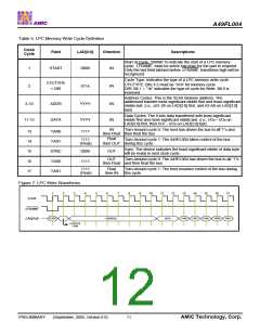
Table 5: LPC Memory Write Cycle Definition
Clock
Cycle
Field
LAD[3:0]
Direction
Descriptions
Start of Cycle: “0000b” to indicate the start of a LPC memory
cycle. LFRAME must be active low (low) for the part to respond.
Only the last field latched before LFRAME transitions high will be
recognized.
1
START
0000
IN
Cycle Type: Indicates the type of a LPC memory write cycle.
CYCTYPE
+ DIR
CYCTYPE: Bits 3-2 must be “01b” for memory cycle.
DIR: Bit 1 = “1b” indicates the type of cycle for Write. Bit 0 is
reserved.
2
011x
IN
IN
Address Cycles: This is the 32-bit memory address. The
addressed transfer most-significant nibble first and least-significant
nibble last. (i.e., a31-28 on LAD[3:0] first, and A3-A0 on LAD[3:0]
last).
3-10
ADDR
DATA
YYYY
Data Cycles: The 8-bits data transferred with least-significant
nibble first and most-significant nibble last. (i.e., I/O3 – I/O0 on
LAD[3:0] first, then I/O7 – I/O4 on LAD[3:0] last).
11-12
YYYY
1111
IN
IN
Turn-Around cycle 0: The host has driven the bus to all”1”s and
13
14
15
16
17
TAR0
TAR1
SYNC
TAR0
TAR1
then Float then float the bus.
Float
then OUT during this cycle.
1111
(Float)
Turn-Around cycle 1: The A49FL004 takes control of the bus
Sync: The device indicates the least-significant nibble of data byte
will be ready in next clock cycle.
0000
1111
OUT
OUT
Turn-Around cycle 0: The A49FL004 has driven the bus to all “1”s
then Float and then float the bus.
1111
(Float)
Float
then IN
Turn-Around cycle 1: The host resumes control of the bus during
this cycle.
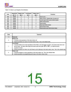
Figure 7: LPC Write Waveforms
1
2
3
4
5
6
7
8
9
10
11
12
13
14
15
16
17
LCLK
LFRAME
LAD[3:0]
START
ADDRESS
DATA
TAR0
TAR1
SYNC
TAR0
TAR1
CYCTYPE
+ DIR
PRELIMINARY
(September, 2005, Version 0.0)
11
AMIC Technology, Corp.

 AMICC [ AMIC TECHNOLOGY ]