A49FL004
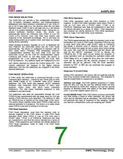
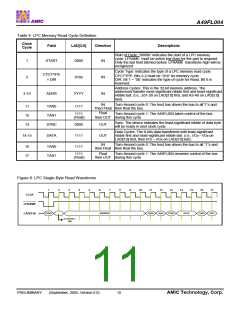
Table 4: LPC Memory Read Cycle Definition
Clock
Cycle
Field
LAD[3:0]
Direction
Descriptions
Start of Cycle: “0000b” indicates the start of a LPC memory
cycle.LFRAME must be active low (low) for the part to respond.
Only the last field latched before LFRAME transitions high will be
recognized.
1
START
0000
IN
Cycle Type: Indicates the type of a LPC memory read cycle.
CYCTYPE
+ DIR
CYCTYPE: Bits 3-2 must be “01b” for memory cycle.
DIR: Bit 1 = “0b” indicates the type of cycle for Read. Bit 0 is
reserved.
2
010x
IN
Address Cycles: This is the 32-bit memory address. The
addressed transfer most-significant nibble first and least-significant
nibble last. (i.e., a31-28 on LAD[3:0] first, and A3-A0 on LAD[3:0]
last).
3-10
ADDR
YYYY
1111
IN
IN
Turn-Around cycle 0: The host has driven the bus to all”1”s and
11
12
13
TAR0
TAR1
SYNC
Then Float then float the bus.
Float
then OUT during this cycle.
1111
(Float)
Turn-Around cycle 1: The A49FL004 takes control of the bus
Sync: The device indicates the least-significant nibble of data byte
will be ready in next clock cycle.
0000
1111
1111
OUT
Data Cycles: The 8-bits data transferred with least-significant
nibble first and most-significant nibble last. (i.e., I/O3 – I/O0 on
LAD[3:0] first, then I/O7 – I/O4 on LAD[3:0] last).
14-15
DATA
OUT
IN
Turn-Around cycle 0: The host has driven the bus to all “1”s and
then Float then float the bus.
16
17
TAR0
TAR1
1111
(Float)
Float
Turn-Around cycle 1: The A49FL004 resumes control of the bus
then OUT during this cycle.
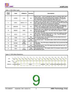
Figure 6: LPC Single-Byte Read Waveforms
1
2
3
4
5
6
7
8
9
10
11
12
13
14
15
16
17
LCLK
LFRAME
LAD[3:0]
START
ADDRESS
TAR0
TAR1
SYNC
DATA
TAR0
TAR1
CYCTYPE +
DIR
PRELIMINARY
(September, 2005, Version 0.0)
10
AMIC Technology, Corp.

 AMICC [ AMIC TECHNOLOGY ]