A49FL004
the rising edge of the clock. The pulse of LFRAME signal
inserted for one or more clocks indicates the start of a LPC
memory read or write cycle.
LPC MODE SELECTION
The A49FL004 can operate in two configurable interfaces:
The In-System Hardware interface and Address/Address
Multiplexed (A/A Mux) interface controlled by IC pin. If the IC
pin is set to logic high (VIH), the devices enter into A/A Mux
interface mode. If the IC pin is set logic low (VIL), the devices
will be in in-system hardware interface mode. During the in-
system hardware interface mode, the devices can
automatically detect the Firmware Hub (FWH) or Low Pin
Count (LPC) memory cycle sent from host system and
response to the command accordingly. The IC pin must be
setup during power-up or system reset, and stays no change
during device operation.
Once the LPC memory cycle is started, asserted by
LFRAME , a START value “0000b” is expected by the device
as a valid command cycle.
Then a CYCTYPE + DIR value (“010xb” for memory read
cycle or “011xb” for memory write cycle) is used to indicates
the type of memory cycle. Refer to Table 4 and 5 for LPC
Memory Read and Write Cycle Definition.
There are 8 clock fields in a LPC memory cycle that gives a
32 bit memory address A31 - A0 through LAD[3:0] with the
most-significant nibble first. The memory space of A49FL004
is mapped directly to top of 4 Gbyte system memory space.
See Figure 8 for System Memory Map.
When working in-system, typically on a PC or Notebook for
non Intel Platform, the A49FL004 is connected to the host
system through a 5-pin communication interface operated
based on a 33-MHz synchronous clock. The 5-pin interface is
The A49FL004 is mapped to the address location of
(FFFFFFFFh - FFF80000h), the A31- A19 must be loaded
with “1” to select and activate the device during a LPC
memory operation. Only A18 - A0 is used to decode and
access the 512 KByte memory.
defined as LAD[3:0] and LFRAME pins under LPC mode for
easy understanding as to those existing compatible products.
When working off-system, typically on
Programmer, the device is operated through 11-pin
multiplexed address - A[10:0] and 8-pin data I/O - I/O[7:0]
interfaces. The memory addresses of device are input
through two bus cycles as row and column addresses
a
EPROM
LPC Abort Operation
controlled by a R/C pin.
The LFRAME is driven low for one or more clock cycles
during a LPC cycle, the cycle will be terminated and the
device will wait for the ABORT command. The host may drive
the LAD[3:0] with “1111b” (ABORT command) to return the
device to the ready mode. If abort occurs during a Write
operation such as checking the operation status with
LPC MODE OPERATION
In LPC mode, the A49FL004 is connected through a 5-pin
communication interface - LAD[3:0] and LFRAME pins to
work with non Intel® Family of South Bridge chipset
platforms. The LPC mode also supports JEDEC standard
Software Data Protection (SDP) product ID entry, byte
program, sector erase, and block erase command sequences.
The chip erase command sequence is only available in A/A
Mux mode.
Data Polling (I/O7) or Toggle Bit (I/O6) pins, the read status
cycle will be aborted but the internal program or erase
operation will not be affected. In this case, only the reset
operation initiated by RST or INIT pin can terminate the
write operation.
Response TO Invalid Fields
The addresses and data are transmitted through the 4-bit
LAD[3:0] bus synchronized with the input clock on CLK pin
during a LAD memory cycle operation. The address or data
on LAD[3:0] bus is latched on the rising edge of the clock.
During LPC operations, the A49FL004 will not explicitly
indicate that it has received invalid field sequences. The
responses to specific invalid fields or sequence is as follows:
The pulse of LFRAME pin is inserted for one clock indicates
the start of a LPC memory read or memory write cycle. The
address or data on LAD[3:0] is latched on the rising edge of
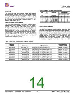
Address out of range: The A49FL004 will only response to
address range as specified in Table 9. Address A22 has the
special function of directing reads and writes to the flash
memory (A22=1) or to the register space (A22=0).
CLK. The device enters standby mode when LFRAME is
high and no internal operation is in progress. The device is in
ready mode when LFRAME is low and no activity is on the
LPC bus.
ID mismatch: The A49FL004 will compare ID bits in the
address field with the hardware strapping. If there is a
mismatch, the device will ignore the cycle.
LPC Mode Memory Read/Write Operation
In LPC mode, the A49FL004 uses the 5-pin LPC interface
includes 4-bit LAD[3:0] and LFRAME pins to communicate
with the host system. The addresses and data are
transmitted through the 4-bit LAD[3:0] bus synchronized with
the input clock on CLK pin during a LPC memory cycle
operation. The address or data on LAD[3:0] bus is latched on
PRELIMINARY
(September, 2005, Version 0.0)
9
AMIC Technology, Corp.

 AMICC [ AMIC TECHNOLOGY ]