A49FL004
FWH MODE SELECTION
FWH Write Operation
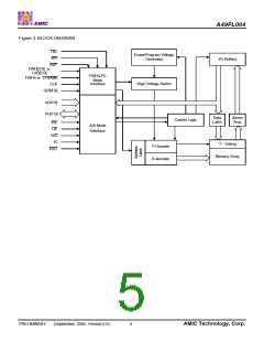
The A49FL004 can operate in two configurable interfaces:
The In-System Hardware interface and Address/Address
Multiplexed (A/A Mux) interface controlled by IC pin. If the IC
pin is set to logic high (VIH), the devices enter into A/A Mux
interface mode. If the IC pin is set logic low (VIL), the device
will be in in-system hardware interface mode. During the in-
system hardware interface mode, the device can
automatically detect the Firmware Hub (FWH) or Low Pin
Count (LPC) memory cycle sent from host system and
response to the command accordingly. The IC pin must be
setup during power-up or system reset, and stays no change
during device operation.
FWH Write operations write the FWH Interface or FWH
registers. A valid FWH Write operation starts when FWH4 is
Low as CLK rises and a START value “1110b” is on
FWH[3:0]. Addresses and data are transferred to and from
the device decided by a series of “fields”. Field sequences
and contents are strictly defined for FWH Write operations.
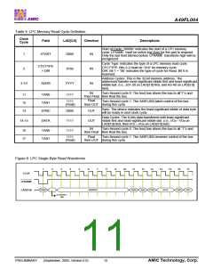
Refer to Table 3 for FWH Write Cycle Definition.
FWH Abort Operation
The FWH4 signal indicates the start of a memory cycle or the
termination of a cycle in FWH mode. Asserting FWH4 for one
or more clock cycle with a valid START value on FWH[3:0]
will initiate a memory read or memory write cycle. If the
FWH4 is driven low again for one or more clock cycles during
this cycle, this cycle will be terminated and the device will
wait for the ABORT command “1111b” to release the
FWH[3:0] bus. If the abort occurs during the program or
erase operation such as checking the operation status with
When working in-system, typically on a PC or Notebook for
Intel Platform, the A49FL004 enters into the FWH mode
automatically. The device is configured to interface with its
host using Intel’s Firmware Hub proprietary protocol.
Communication between the host (Intel ICH) and the
A49FL004 occurs via the 4-bit I/O communication signal,
FWH[3:0] and FWH4. In A/A Mux mode, the device is
programmed via 11-bit address A[10:0] and 8-pin data
I/O[7:0] interfaces. The address inputs are multiplexed in row
Data Polling (I/O7) or Toggle Bit (I/O6) pins, the read status
cycle will be aborted but the internal program or erase
operation will not be affected. Only the reset operation
and column selected by column the control signal R/C . The
column addresses are mapped to the higher internal
addresses, and the row addresses are mapped to the lower
internal addresses.
initiated by RST or INIT pin can terminate the program or
erase operation.
Response To Invalid Fields
FWH MODE OPERATION
During FWH operations, the device will not explicitly indicate
that it has received invalid field sequences. The response to
specific invalid fields or sequences is as follows:
In FWH mode, the A49FL004 is connected through a 5-pin
communication interface - FWH[3:0] and FWH4 pins to work
with Intel® Family of I/O Controller Hubs (ICH) chipset
platforms. The FWH mode also supports JEDEC standard
Software Data Protection (SDP) product ID entry, byte
program, sector erase, and block erase command
sequences. The chip erase command sequence is only
available in A/A Mux mode.
Address out range: The FWH address sequence is 7 fields
long (28 bits), but only the last five address fields (20 bits)
will be decoded by A49FL004. Address A22 has the special
function of directing reads and writes to the flash memory
(A22=1) or to the register space (A22=0).
The addresses and data are transmitted through the 4-bit
FWH[3:0] bus synchronized with the input clock on CLK pin
during a FWH memory cycle operation. The address or data
on FWH[3:0] bus is latched on the rising edge of the clock.
The device enters standby mode when FWH4 is high and no
internal operation is in progress. The device is in ready mode
when FWH4 is low and no activity is on the bus.
Invalid IMSIZE Field: If the FWH device receives and invalid
size field during a Read or Write operation, the device will
reset and no operation will be attempted. The A49FL004 will
not generate any kind of response in this situation. Invalid
size field for a Read/Write cycles are anything but “0000b”.
FWH Read Operation
FWH Read Operations read from the memory cells or
specific registers in the FWH device. A valid FWH Read
operation starts when FWH4 is Low as CLK rises and a
START value “1101b” is on FWH[3:0]. Addresses and data
are transferred to and from the device decided by a series of
“fields”. Field sequences and contents are strictly defined for
FWH Read Operations. Refer to Table 2 for FWH Read
Cycle definition.
PRELIMINARY
(September, 2005, Version 0.0)
6
AMIC Technology, Corp.

 AMICC [ AMIC TECHNOLOGY ]