A49FL004
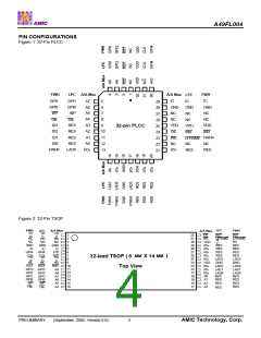
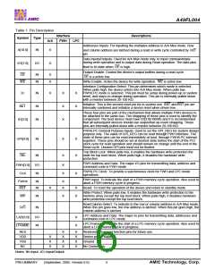
Table 1: Pin Description
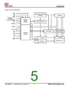
Interface
FWH
Descriptions
Symbol Type
A/A
LPC
Addresses Inputs: For inputting the multiplex address in A/A Mux mode. Row
A[10:0]
I/O[7:0]
IN
X
X
and column address are latched during a read or write cycle controlled by R/C
pin.
Data Inputs/Outputs: Used for A/A Mux mode only, to input command/data
during write operation and to output data during Read operation. The data pins
I/O
float to tri-state when OE is high.
Output Enable: Control the device’s output buffers during a read cycle.
OE is a active low.
OE
IN
IN
X
X
WE
Write Enable: Active the device for write operation. WE is active low.
Interface Configuration Select: This pin determines which mode is selected.
When pulls high, the device enters into A/A Mux mode. When pulls low,
FWH/LPC mode is selected. This pin must be setup during power-up or system
reset, and stays no change during operation. This pin is internally pulled down
with a resistor between 20-100 KΩ.
IC
IN
IN
IN
X
X
X
X
X
X
Initialize: This is the second reset pin for in-system use. INIT andRST pin are
internally combined and initialize a device reset when driven low.
INIT
These four pins are part of the mechanism that allows multiple FWH devices to
be attached to the same bus. The strapping of these pins is used to identify the
component. The boot device must have ID[3:0]=0000b and it is recommended
that all subsequent devices should use sequential up-count strapping. These
pins are internally pulled-down with a resistor between 20-100 KΩ.
ID[3:0]
FWH/LPC General Purpose Inputs: Used to set the GPI_REG for system design
purpose only. The value of GPI_REG can be read through FWH interface. The
state of these pins can be read immediately at boot, through FWH/LPC internal
registers. These pins should be set at desired state before the start of the PCI
clock cycle for read operation and should remain on change until the end of the
Read cycle. Unused GPI pins must not be floated.
GPI[4:0]
TBL
IN
IN
X
X
X
X
Top Block Lock: When pulls low, it enables the hardware write protection the
state for top boot block. When pulls high, it disables the hardware write
protection.
FWH Address and Data: The major I/O pins for transmitting data, address and
command code in FWH mode.
FWH[3:0]
CLK
I/O
IN
X
X
FWH/LPC Clock: To provide a synchronous clock for FWH and LPC mode
operations.
X
FWH Input: To indicate the start of a FWH memory cycle operation. Also used to
abort a FWH memory cycle in progress.
FWH4
RST
IN
IN
X
X
X
X
X
Reset: To reset the operation of the device and return to standby mode.
Write Protect: When pulls low, it enables the hardware write protection to the
memory array except the top boot block. When pulls high, it disables hardware
write protection except the top boot block.
WP
R/C
IN
IN
X
Row/Column Select: To indicate to the row or column address in A/A Mux mode.
When this pin goes low, the row address is latched. When this pin goes high, the
column address is latched.
LPC Address and Data: The major i/o pins for transmitting data, addresses and
command code in LPC mode.
LAD[3:0]
LFRAME
I/O
IN
X
X
LPC Frame: To indicate the start of a LPC memory cycle operation. Also used to
abort a LPC memory cycle in progress.
RES
VDD
VSS
NC
X
X
X
X
X
X
X
X
Reserved. Reserved function pins for future use.
X
X
X
Device power supply.
Ground.
No Connection.
Notes: IN=Input, I/O=Input/Output.
PRELIMINARY
(September, 2005, Version 0.0)
5
AMIC Technology, Corp.

 AMICC [ AMIC TECHNOLOGY ]