P R E L I M I N A R Y
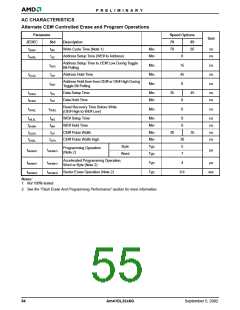
AC CHARACTERISTICS
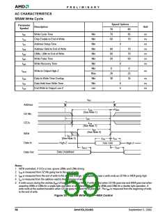
SRAM Write Cycle
Speed Options
Parameter
Description
Symbol
Unit
70
85
85
70
tWC
tCw
tAS
Write Cycle Time
Min
Min
Min
Min
Min
Min
Min
Min
Max
Min
Min
min
70
60
ns
ns
ns
ns
ns
ns
ns
Chip Enable to End of Write
Address Setup Time
0
0
tAW
tBW
tWP
tWR
Address Valid to End of Write
UB#s, LB#s to End of Write
Write Pulse Time
60
60
50
70
70
60
Write Recovery Time
0
0
tWHZ
Write to Output High-Z
ns
20
30
25
35
tDW
tDH
tOW
Data to Write Time Overlap
Data Hold from Write Time
End Write to Output Low-Z
ns
ns
ns
0
5
tWC
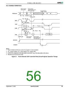
Address
tWR
tCW
(See Note 1)
CE1#s
CE2s
tAW
tCW
(See Note 1)
tWP
(See Note 4)
WE#
tAS
(See Note 3)
tDH
tDW
Data In
Data Out
High-Z
Data Valid
High-Z
tWHZ
tOW
Data Undefined
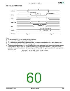
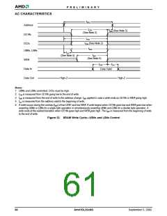
Notes:
1. WE# controlled, if CIOs is low, ignore UB#s and LB#s timing.
2. tCW is measured from CE1#s going low to the end of write.
3. tWR is measured from the end of write to the address change. tWR applied in case a write ends as CE1#s or WE# going high.
4. tAS is measured from the address valid to the beginning of write.
5. A write occurs during the overlap (tWP) of low CE#1 and low WE#. A write begins when CE1#s goes low and WE# goes low when
asserting UB#s or LB#s for a single byte operation or simultaneously asserting UB#s and LB#s for a double byte operation. A
write ends at the earliest transition when CE1#s goes high and WE# goes high. The tWP is measured from the beginning of write
to the end of write.
Figure 30. SRAM Write Cycle—WE# Control
58
Am41DL32x8G
September 5, 2002

 AMD [ AMD ]