P R E L I M I N A R Y
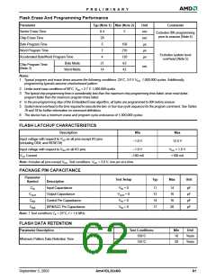
Flash Erase And Programming Performance
Parameter
Typ (Note 1) Max (Note 2)
Unit
sec
sec
µs
Comments
Sector Erase Time
0.4
28
5
5
Excludes 00h programming
prior to erasure (Note 4)
Chip Erase Time
Byte Program Time
Word Program Time
Accelerated Byte/Word Program Time
150
210
120
63
7
µs
Excludes system level
overhead (Note 5)
4
µs
Byte Mode
Word Mode
21
14
Chip Program Time
(Note 3)
sec
42
Notes:
1. Typical program and erase times assume the following conditions: 25°C, 3.0 V VCC, 1,000,000 cycles. Additionally,
programming typicals assume checkerboard pattern.
2. Under worst case conditions of 90°C, VCC = 2.7 V, 1,000,000 cycles.
3. The typical chip programming time is considerably less than the maximum chip programming time listed, since most bytes
program faster than the maximum program times listed.
4. In the pre-programming step of the Embedded Erase algorithm, all bytes are programmed to 00h before erasure.
5. System-level overhead is the time required to execute the two- or four-bus-cycle sequence for the program command. See Tables
16 and 18 for further information on command definitions.
6. The device has a minimum erase and program cycle endurance of 1,000,000 cycles.
FLASH LATCHUP CHARACTERISTICS
Description
Min
Max
Input voltage with respect to VSS on all pins except I/O pins
(including OE#, and RESET#)
–1.0 V
12.5 V
Input voltage with respect to VSS on all I/O pins
VCC Current
–1.0 V
VCC + 1.0 V
+100 mA
–100 mA
Note: Includes all pins except VCC. Test conditions: VCC = 3.0 V, one pin at a time.
PACKAGE PIN CAPACITANCE
Parameter
Symbol
Test Setup
Typ
Max
Unit
Description
CIN
Input Capacitance
VIN = 0
VOUT = 0
VIN = 0
VIN = 0
11
12
14
17
14
16
16
20
pF
pF
pF
pF
COUT
CIN2
Output Capacitance
Control Pin Capacitance
WP#/ACC Pin Capacitance
CIN3
Note: 7.Test conditions TA = 25°C, f = 1.0 MHz.
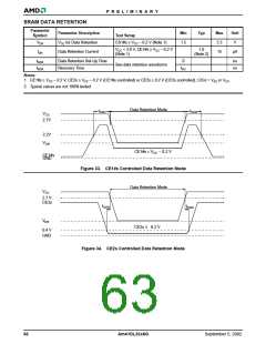
FLASH DATA RETENTION
Parameter Description
Test Conditions
Min
10
Unit
Years
Years
150°C
125°C
Minimum Pattern Data Retention Time
20
September 5, 2002
Am41DL32x8G
61

 AMD [ AMD ]