P R E L I M I N A R Y
AC CHARACTERISTICS
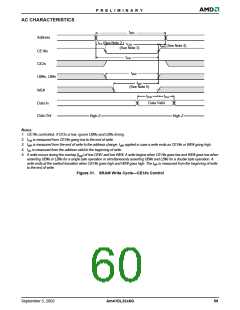
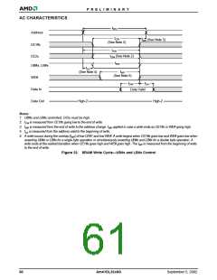
tWC
Address
tAS (See Note 2 )
tCW
tWR (See Note 4)
(See Note 3)
CE1#s
tAW
CE2s
tBW
UB#s, LB#s
tWP
(See Note 5)
WE#
tDW
tDH
Data Valid
Data In
Data Out
High-Z
High-Z
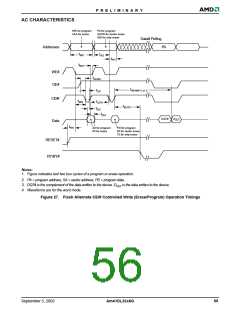
Notes:
1. CE1#s controlled, if CIOs is low, ignore UB#s and LB#s timing.
2. tCW is measured from CE1#s going low to the end of write.
3. tWR is measured from the end of write to the address change. tWR applied in case a write ends as CE1#s or WE# going high.
4. tAS is measured from the address valid to the beginning of write.
5. A write occurs during the overlap (tWP) of low CE#1 and low WE#. A write begins when CE1#s goes low and WE# goes low when
asserting UB#s or LB#s for a single byte operation or simultaneously asserting UB#s and LB#s for a double byte operation. A
write ends at the earliest transition when CE1#s goes high and WE# goes high. The tWP is measured from the beginning of write
to the end of write.
Figure 31. SRAM Write Cycle—CE1#s Control
September 5, 2002
Am41DL32x8G
59

 AMD [ AMD ]